TDA8954TH/N1,118 NXP Semiconductors, TDA8954TH/N1,118 Datasheet - Page 24
TDA8954TH/N1,118
Manufacturer Part Number
TDA8954TH/N1,118
Description
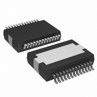
IC AMP AUDIO CLASS D 24HSOP
Manufacturer
NXP Semiconductors
Type
Class Dr
Datasheet
1.TDA8954THN1118.pdf
(46 pages)
Specifications of TDA8954TH/N1,118
Output Type
1-Channel (Mono) or 2-Channel (Stereo)
Max Output Power X Channels @ Load
420W x 1 @ 8 Ohm; 235W x 2 @ 3 Ohm
Voltage - Supply
±12.5 V ~ 42.5 V
Features
Depop, Differential Inputs, Mute, Short-Circuit and Thermal Protection, Standby
Mounting Type
Surface Mount
Package / Case
24-HSOP
Lead Free Status / RoHS Status
Lead free / RoHS Compliant
Other names
568-5076-2


NXP Semiconductors
TDA8954_1
Product data sheet
14.3.2 Bridge-Tied Load (BTL)
14.4 External clock
14.5 Heatsink requirements
Maximum output power:
Maximum output current internally limited to 12 A:
Where:
Remark: Note that I
of the current through the load and the ripple current. The value of the ripple current is
dependent on the coil inductance and the voltage drop across the coil.
To ensure duty cycle-independent operation, the external clock frequency is divided by
two internally. The external clock frequency is therefore twice the internal clock frequency
(typically 2 × 335 kHz = 670 kHz).
If several Class D amplifiers are used in a single application, it is recommended that all
the devices run at the same switching frequency. This can be achieved by connecting the
OSC pins together and feeding them from an external oscillator. When using an external
oscillator, it is necessary to force pin OSC to a DC level above SGND. This disables the
internal oscillator and causes the PWM to switch at half the external clock frequency.
The internal oscillator requires an external resistor R
and pin OSCREF. R
The noise generated by the internal oscillator is supply voltage dependent. An external
low-noise oscillator is recommended for low-noise applications running at high supply
voltages.
An external heatsink must be connected to the TDA8954.
Equation 5
of TFB and total thermal resistance from junction to ambient.
P
I
o peak
•
•
•
•
•
•
•
o 0.5%
(
(
P
R
R
R
R
t
f
w(min)
osc
o(0.5 %)
L
DSon(hs)
DSon(ls)
s(L)
: load impedance
)
: oscillator frequency
)
=
: series impedance of the filter coil
=
: minimum pulse width (typical 150 ns, temperature dependent)
--------------------------------------------------------------------------------------------- -
R
defines the relationship between maximum power dissipation before activation
(
-----------------------------------------------------------------------------------------------------------------------------------------------------------------------------
: output power at the onset of clipping
: low-side R
V
L
------------------------------------------------------------------ -
R
: high-side R
DD
+
L
+
(
R
–
R
DSon hs
V
DSon hs
o(peak)
OSC
SS
Rev. 01 — 24 December 2009
)
(
(
×
DSon
R
must be removed when using an external oscillator.
)
(
DSon
L
)
1 t
should be less than 12 A; see
+
+
–
R
of power stage output DMOS (temperature dependent)
R
DSon ls
of power stage output DMOS (temperature dependent)
w min
DSon ls
(
( )
( )
)
×
)
×
+
0.5f
(
2R
V
2R
osc
DD
s L ( )
L
)
–
V
SS
)
OSC
×
2 × 210 W class-D power amplifier
(
1 t
, connected between pin OSC
Section
–
w min
(
)
8.4.2. I
×
0.5f
TDA8954
© NXP B.V. 2009. All rights reserved.
osc
o(peak)
)
2
is the sum
24 of 46
(3)
(4)
Related parts for TDA8954TH/N1,118
Image
Part Number
Description
Manufacturer
Datasheet
Request
R

Part Number:
Description:
2 ? 210 W Class-d Power Amplifier
Manufacturer:
NXP Semiconductors
Datasheet:
Part Number:
Description:
The TDA8954 is a stereo or mono high–efficiency Class D audio power amplifier in asingle IC featuring low power dissipation
Manufacturer:
NXP Semiconductors
Datasheet:
Part Number:
Description:
NXP Semiconductors designed the LPC2420/2460 microcontroller around a 16-bit/32-bitARM7TDMI-S CPU core with real-time debug interfaces that include both JTAG andembedded trace
Manufacturer:
NXP Semiconductors
Datasheet:

Part Number:
Description:
NXP Semiconductors designed the LPC2458 microcontroller around a 16-bit/32-bitARM7TDMI-S CPU core with real-time debug interfaces that include both JTAG andembedded trace
Manufacturer:
NXP Semiconductors
Datasheet:
Part Number:
Description:
NXP Semiconductors designed the LPC2468 microcontroller around a 16-bit/32-bitARM7TDMI-S CPU core with real-time debug interfaces that include both JTAG andembedded trace
Manufacturer:
NXP Semiconductors
Datasheet:
Part Number:
Description:
NXP Semiconductors designed the LPC2470 microcontroller, powered by theARM7TDMI-S core, to be a highly integrated microcontroller for a wide range ofapplications that require advanced communications and high quality graphic displays
Manufacturer:
NXP Semiconductors
Datasheet:
Part Number:
Description:
NXP Semiconductors designed the LPC2478 microcontroller, powered by theARM7TDMI-S core, to be a highly integrated microcontroller for a wide range ofapplications that require advanced communications and high quality graphic displays
Manufacturer:
NXP Semiconductors
Datasheet:
Part Number:
Description:
The Philips Semiconductors XA (eXtended Architecture) family of 16-bit single-chip microcontrollers is powerful enough to easily handle the requirements of high performance embedded applications, yet inexpensive enough to compete in the market for hi
Manufacturer:
NXP Semiconductors
Datasheet:
Part Number:
Description:
The XA-S3 device is a member of Philips Semiconductors? XA(eXtended Architecture) family of high performance 16-bitsingle-chip microcontrollers
Manufacturer:
NXP Semiconductors
Datasheet:

Part Number:
Description:
The NXP BlueStreak LH75401/LH75411 family consists of two low-cost 16/32-bit System-on-Chip (SoC) devices
Manufacturer:
NXP Semiconductors
Datasheet:
Part Number:
Description:
The NXP LPC3130/3131 combine an 180 MHz ARM926EJ-S CPU core, high-speed USB2
Manufacturer:
NXP Semiconductors
Datasheet:
Part Number:
Description:
The NXP LPC3141 combine a 270 MHz ARM926EJ-S CPU core, High-speed USB 2
Manufacturer:
NXP Semiconductors
Part Number:
Description:
The NXP LPC3143 combine a 270 MHz ARM926EJ-S CPU core, High-speed USB 2
Manufacturer:
NXP Semiconductors