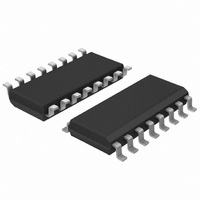
TDA8543T/N1,518 NXP Semiconductors, TDA8543T/N1,518 Datasheet - Page 6

TDA8543T/N1,518
Manufacturer Part Number
TDA8543T/N1,518
Description
IC AMP AUDIO PWR 2.2W AB 16SOIC
Manufacturer
NXP Semiconductors
Type
Class ABr
Datasheet
1.TDA8543TN1518.pdf
(19 pages)
Specifications of TDA8543T/N1,518
Output Type
1-Channel (Mono)
Package / Case
16-SOIC (3.9mm Width)
Max Output Power X Channels @ Load
2.2W x 1 @ 8 Ohm
Voltage - Supply
2.2 V ~ 18 V
Features
Depop, Mute, Short-Circuit and Thermal Protection, Standby
Mounting Type
Surface Mount
Product
Class-AB
Output Power
2.2 W
Available Set Gain
30 dB
Thd Plus Noise
0.15 %
Operating Supply Voltage
5 V
Supply Current
8 mA
Maximum Power Dissipation
1.2 W
Maximum Operating Temperature
+ 85 C
Mounting Style
SMD/SMT
Audio Load Resistance
16 Ohms
Input Bias Current (max)
0.5 uA
Input Signal Type
Differential or Single
Minimum Operating Temperature
- 40 C
Output Signal Type
Differential, Single
Supply Type
Single
Supply Voltage (max)
18 V
Supply Voltage (min)
2.2 V
Operational Class
Class-AB
Audio Amplifier Output Configuration
1-Channel Mono
Output Power (typ)
2.2x1@8OhmW
Audio Amplifier Function
Speaker
Total Harmonic Distortion
0.15@8Ohm@0.5W%
Single Supply Voltage (typ)
5V
Dual Supply Voltage (typ)
Not RequiredV
Power Supply Requirement
Single
Power Dissipation
1.2W
Rail/rail I/o Type
No
Single Supply Voltage (min)
2.2V
Single Supply Voltage (max)
18V
Dual Supply Voltage (min)
Not RequiredV
Dual Supply Voltage (max)
Not RequiredV
Operating Temp Range
-40C to 85C
Operating Temperature Classification
Industrial
Mounting
Surface Mount
Pin Count
16
Lead Free Status / RoHS Status
Lead free / RoHS Compliant
Lead Free Status / RoHS Status
Lead free / RoHS Compliant, Lead free / RoHS Compliant
Other names
568-2380-2
935227370518
TDA8543TD-T
935227370518
TDA8543TD-T
NXP Semiconductors
DC CHARACTERISTICS
V
Notes
1. With a load connected at the outputs the quiescent current will increase, the maximum of this increase being equal
2. The DC output voltage with respect to ground is approximately 0.5 × V
AC CHARACTERISTICS
V
specified.
1997 Jun 12
V
I
I
V
⎪V
I
V
I
P
THD
G
Z
V
SVRR
V
CC
q
stb
IN+
MODE
CC
i
CC
O
MODE
o
no
o
2 W BTL audio amplifier
v
OUT+
to the DC output offset voltage divided by R
, I
SYMBOL
= 5 V; T
= 5 V; T
SYMBOL
IN−
− V
OUT−
amb
amb
= 25 °C; R
⎪ differential output voltage offset
= 25 °C; R
supply voltage
quiescent current
standby current
DC output voltage
input bias current
input voltage mode select
input current mode select
output power
total harmonic distortion
closed loop voltage gain
differential input impedance
noise output voltage
supply voltage ripple rejection
output voltage in mute condition note 5
L
L
PARAMETER
= 8 Ω; V
= 8 Ω; f = 1 kHz; V
PARAMETER
MODE
= 0 V; G = 20 dB; measured in test circuit Fig.4; unless otherwise specified.
MODE
L
.
= 0 V; G = 20 dB; measured in test circuit Fig.4; unless otherwise
operating
R
V
note 2
operating
mute
standby
0 < V
THD = 10%;
THD = 0.5%;
P
note 1
note 2
note 3
note 4
MODE
L
o
CONDITIONS
V
V
V
V
V
V
= ∞; note 1
= 0.5 W
CC
CC
CC
CC
CC
CC
MODE
6
CONDITIONS
= 5 V; R
= 7.5 V; R
= 9 V; R
= 5 V; R
= 7.5 V; R
= 9 V; R
= V
CC
< V
CC
L
L
L
L
= 8 Ω
= 16 Ω
= 8 Ω
= 16 Ω
L
L
= 8 Ω
= 8 Ω
2.2
−
−
−
−
−
0
1.5
V
−
CC
CC
MIN.
.
− 0.5 −
1
−
−
0.6
−
−
−
6
−
−
50
40
−
MIN.
5
8
−
2.2
−
−
−
−
−
TYP.
0.9
1.2
2.2
2.0
1.7
1.4
0.15
−
100
−
−
−
−
TYP.
18
12
10
−
50
500
0.5
V
V
20
Product specification
CC
CC
MAX.
−
−
−
−
−
−
0.3
30
−
100
−
−
200
MAX.
− 1.5 V
TDA8543
V
mA
μA
V
mV
nA
V
V
μA
W
W
W
W
W
W
%
dB
kΩ
μV
dB
dB
μV
UNIT
UNIT


