MAX9744ETH+ Maxim Integrated Products, MAX9744ETH+ Datasheet - Page 18
MAX9744ETH+
Manufacturer Part Number
MAX9744ETH+
Description
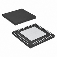
IC AMP AUDIO PWR 22.5W D 44TQFN
Manufacturer
Maxim Integrated Products
Type
Class Dr
Datasheet
1.MAX9744ETH.pdf
(28 pages)
Specifications of MAX9744ETH+
Output Type
2-Channel (Stereo)
Max Output Power X Channels @ Load
22.5W x 2 @ 4 Ohm
Voltage - Supply
4.5 V ~ 14 V
Features
Depop, Mute, Short-Circuit and Thermal Protection, Shutdown, Volume Control
Mounting Type
Surface Mount
Package / Case
44-TQFN Exposed Pad
Product
Class-D
Output Power
20 W
Thd Plus Noise
0.04 %
Supply Current
20 mA
Maximum Power Dissipation
2963 mW
Maximum Operating Temperature
+ 85 C
Audio Load Resistance
4 Ohms
Minimum Operating Temperature
- 40 C
Amplifier Class
D
No. Of Channels
2
Supply Voltage Range
4.5V To 14V
Load Impedance
4ohm
Operating Temperature Range
-40°C To +85°C
Amplifier Case Style
TQFN
Rohs Compliant
Yes
Lead Free Status / RoHS Status
Lead free / RoHS Compliant


20W Stereo Class D Speaker Amplifier
with Volume Control
A write to the MAX9744 includes transmission of a
START condition, the slave address with the R/W bit set
to 0 (see Table 3), one byte of data to the command
register, and a STOP condition. Figure 6 illustrates the
proper format for one frame.
A write to the MAX9744 consists of a 6-step sequence
as seen below:
The command register is used to control the volume
level of the speaker amplifier. The two MSBs (A1 and
A0) are set to 00, while V5–V0 is the data that is written
into the addresses register to set the volume level
(Tables 5 and 6).
Table 5. Data Byte Format
Table 6. Command Register Programming
18
1) The master sends a START condition.
2) The master sends the 7 bits slave ID plus a write
3) The addressed slave asserts an ACK on the data
4) The master sends 8 data bits.
5) The active slave asserts an ACK (or NACK) on the
6) The master generates a stop condition.
D7 (MSB)
A
______________________________________________________________________________________
bit (low).
line.
data line.
00
01
01
0
A1
A
1
XXXXXX
000000
000001
V5–V0
D6
A0
Speaker Volume Control
Volume level (Table 7)
Filterless modulation
Classic PWM
D5
V5
SETTING
Write Byte
D4
V4
The MAX9744 features two output modulation schemes:
filterless modulation or classic PWM, selectable through
the I
to set the output scheme.
When switching between schemes, the output is not
click-and-pop protected. To have click-and-pop protec-
tion when switching between output schemes, the
device must enter shutdown mode and be configured
to the new output scheme before the 220ms startup
sequence is terminated.
Figure 6. Write Byte Format Example
WRITE BYTE FORMAT
S
D3
V3
A
2
C interface. Table 6 shows the register command
10
11
11
0
A
1
SLAVE
SLAVE ADDRESS:
EQUIVALENT TO CHIP-
SELECT LINE OF A
3-WIRE INTERFACE.
7 BITS
ADDRESS
D2
V2
XXXXXX
000100
000101
V5–V0
WR
0
Filterless Modulation/PWM
ACK
D1
V1
Reserved
Increased volume
Decreased volume
DATA BYTE: GIVES A COMMAND.
8 BITS
DATA
SETTING
D0 (LSB)
ACK
V0
P
Related parts for MAX9744ETH+
Image
Part Number
Description
Manufacturer
Datasheet
Request
R

Part Number:
Description:
20w Stereo Class D Speaker Amplifier With Volume Control
Manufacturer:
Maxim Integrated Products, Inc.
Datasheet:

Part Number:
Description:
MAX7528KCWPMaxim Integrated Products [CMOS Dual 8-Bit Buffered Multiplying DACs]
Manufacturer:
Maxim Integrated Products
Datasheet:
Part Number:
Description:
Single +5V, fully integrated, 1.25Gbps laser diode driver.
Manufacturer:
Maxim Integrated Products
Datasheet:
Part Number:
Description:
Single +5V, fully integrated, 155Mbps laser diode driver.
Manufacturer:
Maxim Integrated Products
Datasheet:
Part Number:
Description:
VRD11/VRD10, K8 Rev F 2/3/4-Phase PWM Controllers with Integrated Dual MOSFET Drivers
Manufacturer:
Maxim Integrated Products
Datasheet:
Part Number:
Description:
Highly Integrated Level 2 SMBus Battery Chargers
Manufacturer:
Maxim Integrated Products
Datasheet:
Part Number:
Description:
Current Monitor and Accumulator with Integrated Sense Resistor; ; Temperature Range: -40°C to +85°C
Manufacturer:
Maxim Integrated Products
Part Number:
Description:
TSSOP 14/A�/RS-485 Transceivers with Integrated 100O/120O Termination Resis
Manufacturer:
Maxim Integrated Products
Part Number:
Description:
TSSOP 14/A�/RS-485 Transceivers with Integrated 100O/120O Termination Resis
Manufacturer:
Maxim Integrated Products
Part Number:
Description:
QFN 16/A�/AC-DC and DC-DC Peak-Current-Mode Converters with Integrated Step
Manufacturer:
Maxim Integrated Products
Part Number:
Description:
TDFN/A/65V, 1A, 600KHZ, SYNCHRONOUS STEP-DOWN REGULATOR WITH INTEGRATED SWI
Manufacturer:
Maxim Integrated Products
Part Number:
Description:
Integrated Temperature Controller f
Manufacturer:
Maxim Integrated Products
Part Number:
Description:
SOT23-6/I�/45MHz to 650MHz, Integrated IF VCOs with Differential Output
Manufacturer:
Maxim Integrated Products
Part Number:
Description:
SOT23-6/I�/45MHz to 650MHz, Integrated IF VCOs with Differential Output
Manufacturer:
Maxim Integrated Products
Part Number:
Description:
EVALUATION KIT/2.4GHZ TO 2.5GHZ 802.11G/B RF TRANSCEIVER WITH INTEGRATED PA
Manufacturer:
Maxim Integrated Products