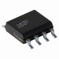
TDA7052BT/N1,118 NXP Semiconductors, TDA7052BT/N1,118 Datasheet - Page 5

TDA7052BT/N1,118
Manufacturer Part Number
TDA7052BT/N1,118
Description
IC AMP AUDIO 1W MONO AB 8SOIC
Manufacturer
NXP Semiconductors
Type
Class ABr
Datasheet
1.TDA7052BTN1118.pdf
(16 pages)
Specifications of TDA7052BT/N1,118
Output Type
1-Channel (Mono)
Package / Case
8-SOIC (3.9mm Width)
Max Output Power X Channels @ Load
550mW x 1 @ 16 Ohm
Voltage - Supply
4.5 V ~ 18 V
Features
Depop, Mute, Short-Circuit and Thermal Protection, Volume Control
Mounting Type
Surface Mount
Product
Class-AB
Output Power
550 mW
Available Set Gain
40.5 dB
Thd Plus Noise
0.3 %
Operating Supply Voltage
5 V, 9 V, 12 V
Maximum Power Dissipation
800 mW
Maximum Operating Temperature
+ 85 C
Mounting Style
SMD/SMT
Audio Load Resistance
8 Ohms
Input Signal Type
Single
Minimum Operating Temperature
- 40 C
Output Signal Type
Differential
Supply Type
Single
Supply Voltage (max)
18 V
Supply Voltage (min)
4.5 V
Lead Free Status / RoHS Status
Lead free / RoHS Compliant
Lead Free Status / RoHS Status
Lead free / RoHS Compliant, Lead free / RoHS Compliant
Other names
935066260118
TDA7052BTD-T
TDA7052BTD-T
TDA7052BTD-T
TDA7052BTD-T
NXP Semiconductors
CHARACTERISTICS
V
Notes
1. With a load connected to the outputs the quiescent current will increase, the maximum value of this increase being
2. The noise output voltage (RMS value) at f = 500 kHz is measured with R
3. The ripple rejection is measured with R
4. The noise output voltage (RMS value) is measured with R
5. The DC volume control can be configured in several ways. Two possible circuits are shown in Figs 14 and 15.
1997 Aug 15
Supply
V
I
Maximum gain (V
P
THD
G
V
V
B
SVRR
⎪ΔV
Z
Mute position
V
DC volume control; note 5
φ
I
SYMBOL
P
q(tot)
4
I
P
O
I
no
O
Mono BTL audio amplifier with DC volume
control
v(max)
= 6 V; V
equal to the DC output offset voltage divided by R
(RMS value) is applied to the positive supply rail.
The circuits at the volume control pin will influence the switch-on and switch-off behaviour and the maximum voltage
gain.
O
⎪
DC
supply voltage
total quiescent current
output power
total harmonic distortion
maximum total voltage gain
input signal handling (RMS value) G
noise output voltage (RMS value)
bandwidth
supply voltage ripple rejection
DC output offset voltage
input impedance (pin 3)
output voltage in mute position
gain control
control current
= 1.4 V; f = 1 kHz; R
TDA7052B
TDA7052BT
TDA7052B
TDA7052BT
4
= 1.4 V)
PARAMETER
L
= 8 Ω; T
S
amb
= 0 Ω and f = 100 Hz to 10 kHz. The ripple voltage V
= 25 °C; unless otherwise specified (see Fig.13).
note 1; R
THD = 10%
P
P
note 2; f = 500 kHz
at −1 dB
note 3
⎪V
note 4; V
V
V
O
O
I
4
v(max)
8
= 1.0 V
= 0 V
= 0.5 W
= 0.25 W
− V
L
.
CONDITIONS
= 0 dB; THD < 1%
5
⎪
4
L
5
≤ 0.4 V;
= ∞
S
= 5 kΩ unweighted.
S
4.5
−
0.9
0.5
−
−
39.5
1.0
−
−
48
−
15
−
68
−20
= 0 Ω and B = 5 kHz.
MIN.
−
9.2
1.0
0.55
0.3
0.3
40.5
−
210
0.02 to 300 −
60
0
20
−
73.5
−25
TYP.
R
Product specification
of 200 mV
TDA7052B
18
13
−
−
1
1
41.5
−
−
−
200
25
30
−
−30
MAX.
V
mA
W
W
%
%
dB
V
μV
kHz
dB
mV
kΩ
μV
dB
μA
UNIT


