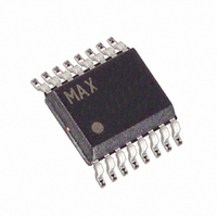
MAX13330GEE/V+T Maxim Integrated Products, MAX13330GEE/V+T Datasheet - Page 10

MAX13330GEE/V+T
Manufacturer Part Number
MAX13330GEE/V+T
Description
IC AMP STEREO HEADPHONE 16-QSOP
Manufacturer
Maxim Integrated Products
Series
DirectDrive™r
Type
Class ABr
Datasheet
1.MAX13330GEEV.pdf
(15 pages)
Specifications of MAX13330GEE/V+T
Output Type
Headphones, 2-Channel (Stereo)
Max Output Power X Channels @ Load
135mW x 2 @ 32 Ohm
Voltage - Supply
4 V ~ 5.5 V
Features
Depop, Short-Circuit Protection, Shutdown
Mounting Type
Surface Mount
Package / Case
16-QSOP
Lead Free Status / RoHS Status
Lead free / RoHS Compliant
Automotive DirectDrive Headphone Amplifiers
with Output Protection and Diagnostics
The MAX13330/MAX13331 provides an analog diag-
nostic output as a fraction of the analog supply voltage
V
condition with the highest priority that is present in the
system, as shown in Table 1. When simultaneous fault
conditions occur on both headphone outputs, the diag-
nostic output will only report the fault condition at OUTR
until it is cleared or removed. Only then will the fault
condition at OUTL be reported at DIAG. Connect DIAG
to a high-impedance input.
Table 1. MAX13330/MAX13331 Diagnostic
Priority
For both headphone outputs, short circuits to V
dynamic and V
soon as the fault condition is removed. Short circuits to
GND occurring when a positive output voltage is pre-
sent on OUTL or OUTR, will result in V
latched until the fault condition is cleared.
When V
gling SHDN low for less than 5µs or initiating a full reset
of the MAX13330/MAX13331. Toggling SHDN low for
less than 5µs will cause the fault to ground to be
cleared without shutting down the device or interrupting
the output state of the amplifiers. A full reset requires
SHDN to be pulled low for more than 50µs. The amplifi-
er outputs will enter high impedance and remain in that
state until the device exits shutdown.
In conventional single-supply audio amplifiers, the out-
put-coupling capacitor is a major contributor of audible
clicks and pops. Upon startup, the amplifier charges
the coupling capacitor to its bias voltage, typically half
the supply. Likewise, on shutdown, the capacitor is dis-
charged to SGND. This results in a DC shift across the
capacitor which appears as an audible transient at the
speaker. Since the MAX13330/MAX13331 does not
require output-coupling capacitors, this problem does
not arise.
10
DD
Three State
. The voltage at DIAG will correspond to the fault
3/4 V
1/2 V
1/4 V
______________________________________________________________________________________
V
V
DIAG
DD
0
DIAG
DD
DD
DD
is latched, it can be cleared by either tog-
DIAG
OUTL Short to V
OUTR Short to V
OUTL Short to SGND
OUTR Short to SGND
No Fault
Shutdown
Click-and-Pop Suppression
will be automatically cleared as
STATE
BAT
BAT
Diagnostic Output
PRIORITY
DIAG
—
3
1
4
2
5
BAT
being
are
Additionally, the MAX13330/MAX13331 feature exten-
sive click-and-pop suppression that eliminates any
audible transient sources internal to the device. The
Power-Up/-Down Transient graph in the Typical
Operating Characteristic s shows that there is minimal
DC shift and no spurious transients at the output upon
startup or shutdown.
In most applications, the output of the preamplifier dri-
ving the MAX13330/MAX13331 has a DC bias of typi-
cally half the supply. At startup, the input-coupling
capacitor is charged to the preamplifier’s DC-bias volt-
age through the feedback resistor of the MAX13330/
MAX13331, resulting in a DC shift across the capacitor
and an audible click/pop. Delaying the rise of SHDN 4
to 5 time constants (80ms to 100ms) based on R
C
this click/pop caused by the input filter.
The MAX13330/MAX13331 feature shutdown control
allowing audio signals to be shut down or muted.
Driving SHDN low disables the amplifiers and the
charge pump, sets the amplifier output impedance to
14kΩ (typ), and reduces the supply current. In shut-
down mode, the supply current is reduced to 2µA. The
charge pump is enabled once SHDN is driven high.
Under normal operating conditions, linear power ampli-
fiers can dissipate a significant amount of power. The
maximum power dissipation for each package is given
in the Absolute Maximum Ratings section under contin-
uous power dissipation or can be calculated by the
following equation:
where T
ture, and θ
°C/W as specified in the Absolute Maximum Ratings
section. The thermal resistance θ
age is 120°C/W.
The MAX13330/MAX13331 have two power dissipation
sources: the charge pump and two amplifiers. If power
dissipation for a given application exceeds the maxi-
mum allowed for a particular package, either reduce
V
temperature, or add heatsinking to the device. Large
output, supply, and ground traces improve the maxi-
mum power dissipation in the package.
DD
IN
, increase load impedance, decrease the ambient
relative to the startup of the preamplifier, eliminates
J(MAX)
JA
P
DISSPKG MAX
is the reciprocal of the derating factor in
Applications Information
is +145°C, T
(
)
=
(
A
T
J MAX
is the ambient tempera-
(
Power Dissipation
θ
JA
JA
)
of the QSOP pack-
−
T
A
)
Shutdown
IN
and


