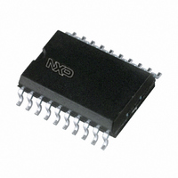
SA5217D/01,112 NXP Semiconductors, SA5217D/01,112 Datasheet - Page 5

SA5217D/01,112
Manufacturer Part Number
SA5217D/01,112
Description
IC POST AMP W/LINK STAT 20SOIC
Manufacturer
NXP Semiconductors
Type
Postamplifierr
Datasheet
1.SA5217D01112.pdf
(12 pages)
Specifications of SA5217D/01,112
Applications
Optical Networks
Mounting Type
Surface Mount
Package / Case
20-SOIC (7.5mm Width)
Lead Free Status / RoHS Status
Lead free / RoHS Compliant
Other names
568-3570-5
935275247112
SA5217D/01
935275247112
SA5217D/01
Philips Semiconductors
AC ELECTRICAL CHARACTERISTICS
Min and Max limits apply over the operating temperature range at V
V
1998 Oct 07
f
V
V
R
C
R
C
R
C
V
V
V
t
t
t
t
CCA
OP
TLH
THL
RFD
PWD
SYMBOL
SYMBOL
INH
INL
HYS
THR
THR
Postamplifier with link status indicator
IN1
IN1
IN8
IN2
OUT2
OUT2
S
= V
CCD
= +5.0V and T
Maximum operating frequency
Maximum Functional A1 input signal (single en-
ded)
Minimum Functional A1 input signal (single-en-
ded)
Minimum Functional A1 input signal (differential)
Minimum input sensitivity for output BER
(single-ended)
Minimum input sensitivity for output BER
(differential)
Input resistance (differential at IN
Input capacitance (differential at IN
Input resistance (differential at IN
Input capacitance (differential at IN
Output resistance (differential at OUT
Output capacitance (differential at OUT
Hysteresis voltage range (single-ended)
Hysteresis voltage range (differential)
Threshold voltage (single-ended)
Threshold voltage (differential)
TTL Output Rise Time 20% to 80%
TTL Output Fall Time 80% to 20%
t
Pulse width distortion of output
TLH
/t
THL
mismatch
A
= 25 C.
PARAMETER
PARAMETER
100 H
100 H
V
+5V
CC
0.1 F
10 F
125
33k
1
2
)
)
1
2
V
)
)
OUT
2
0.1 F
)
2
)
10
10
Figure 3. AC Test Circuit
10
–9
–9
1
2
3
4
5
6
7
8
9
15pF
LED
C
THRESH
GND
FLAG
JAM
V
V
GND
V
CCD
CCA
OUT
PKDET
CCA
Distortion =
A
D
NE5217
400
R
5
= V
PKDET
R
R
R
OUT
OUT
C
(FLAG Low) Test circuit,
C
HYST
RHYST
RHYST
IN
IN
IN
IN
Test circuit, T
AZN
50mV
AZP
TEST CONDITIONS
TEST CONDITIONS
CCD
1B
1A
2B
8B
2A
8A
PRBS = 2
PRBS = 2
PRBS = 2
Test CIrcuit
= +5.0V unless otherwise specified. Typical data applies at
Test Circuit
Test Circuit
Test Circuit
20
19
18
17
16
15
14
13
12
11
Test circuit
=5k R
=4k R
@ 50MHz
P-P
, 1010. . .input
0.1 F
10k
T
T
0.1 F
4k
0.1 F
H
H
THRESH
THRESH
0.1 F
A
A
23
23
23
* T
) T
= 25 C
–1
–1
1
L
L
0.1 F
25
=33k
=33k
10
2
50
SD00356
V
Min
IN
60
LIMITS
1200
2000
TBD
Typ
1.6
4.5
9.5
1.3
1.2
0.1
75
25
10
19
6
3
9
2
2
2
5
Product specification
Max
SA5217
mV
mV
mV
mV
mV
mV
UNIT
UNIT
MHz
V
pF
pF
pF
ns
ns
ns
%
P-P
P-P
P P
P-P
P-P
P-P
P P


