MAX2078CTK+ Maxim Integrated Products, MAX2078CTK+ Datasheet - Page 5

MAX2078CTK+
Manufacturer Part Number
MAX2078CTK+
Description
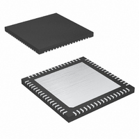
IC FRNT-END ULTRASOUND 8CH 68QFN
Manufacturer
Maxim Integrated Products
Type
Ultrasound Receiversr
Datasheet
1.MAX2078CTK.pdf
(26 pages)
Specifications of MAX2078CTK+
Applications
Medical Ultrasound Imaging, Sonar
Mounting Type
Surface Mount
Package / Case
68-TQFN Exposed Pad
Operating Supply Voltage
3.13 V to 3.47 V
Maximum Operating Temperature
+ 70 C
Mounting Style
SMD/SMT
Minimum Operating Temperature
0 C
Lead Free Status / RoHS Status
Lead free / RoHS Compliant
AC ELECTRICAL CHARACTERISTICS—VGA MODE (continued)
( Typical Application Circuit , V
V/C = 1, NP = 0, PD = 0, D43/D42/D41/D40 = 1/0/1/0 (R
capacitance to GND at each of the VGA differential outputs is 25pF, differential capacitance across VGA outputs is 15pF, R
differential, reference noise less than 10nV/√Hz from 1kHz to 20MHz, DOUT loaded with 10MΩ and 60pF. Typical values are at V
= 3.3V, V
Absolute Gain Error
Input Gain Compression
VGA Gain Response Time
VGA Output Offset Under Pulsed
Overload
Small-Signal Output Noise
Large-Signal Output Noise
Second Harmonic (HD2)
High-Gain IM3 Distortion
Low-Gain IM3 Distortion
Standby Mode Power-Up
Response Time
Standby Mode Power-Down
Response Time
Power-Up Response Time
Power-Down Response Time
Adjacent Channel Crosstalk
Nonadjacent Channel Crosstalk
Phase Matching Between
Channels
CC2
PARAMETER
= 4.75V, T
_______________________________________________________________________________________
A
= +25°C, unless otherwise noted.) (Note 5)
REF
Octal-Channel Ultrasound Front-End
= 2.475V to 2.525V, V
Measured at T
Measured at T
Measured at T
VG+ - VG- = -3V (VGA minimum gain), gain ratio with
330mV
LNA low gain = 12.5dB, VG+ - VG- = -3V (VGA minimum
gain), gain ratio with 600mV
Gain step up (V
44dB, settling time is measured within 1dB final value)
G ai n step d ow n ( V
to 10d B, settl i ng ti m e i s m easur ed w i thi n 1d B fi nal val ue)
Overdrive is ±10mA in clamping diodes, gain at 30dB,
16 pulses at 5MHz, repetition rate 20kHz; offset is
measured at output when RF duty cycle is off
20dB of gain, VG+ - VG- = -0.85V, no input signal
20dB of gain, VG+ - VG- = -0.85V, f
f
V
V
V
V
D43/D42/D41/D40 = 0/0/0/1 (R
12.5dB),V
V
Gain set for 26dB, f
with in 1dB from transition on NP pin
To reach DC current target ±10%
Gain set for 28dB, f
within 1dB from transition on PD
Gain set for 28dB, f
6mW/channel, from transition on PD
V
V
Gain = 28dB, VG+ - VG- = 0.4V, V
f
NOISE
RF
IN
IN
IN
OUT
OUT
OUT
OUT
= 10MHz
= 50mV
= 50mV
= 50mV
= 1V
= 1V
= 1V
= 1V
P-P
= f
RF
/50mV
IN
P-P
P-P
P-P
P-P
P-P
P-P
P-P
= 100mV
+ 1kHz, V
(Note 11)
(Note 11)
differential, f
differential, f
A
A
A
, f
, f
, f
IN
P-P
= +25
= +25
= +25
RF
RF
RF1
I N
= 5mV
CC1
RF
RF
RF
= 2MHz, V
= 5MHz, V
input tones
IN
= 5m V
= 5MHz, f
P-P
CONDITIONS
o
o
o
= 5MHz, V
= 5MHz, V
= 5MHz, DC power reaches
OUT
= 200Ω, LNA gain = 18.5dB), D45/D44 = 1/1 (f
C, VG+ - VG- = -2V
C, VG+ - VG- = 0V
C, VG+ - VG- = +2V
= 3.13V to 3.47V, V
, f
P-P
RF1
RF
RF
P - P
= 1V
P-P
, gain changed from 10dB to
= 10MHz, 28dB of gain
= 10MHz, 28dB of gain
, g ai n chang ed fr om 44d B
with CW Doppler Mixers
OUT
OUT
RF2
= 5MHz, f
IN
/50mV
P-P
OUT
OUT
= 200Ω, LNA gain =
OUT
= 5.01MHz,
= 1V
= 1V
RF
differential
P-P
= 1V
= 1V
= 5MHz,
= 1V
P-P
P-P
RF2
P-P
P-P
CC2
P-P
= 5.01MHz,
, settled
, settled
,
= 4.5V to 5.25V, T
MIN
-52
-50
A
= 0°C to +70°C, V
-64.2
±0.4
±0.4
±0.4
±1.2
TYP
180
C
1.4
0.8
1.4
1.6
-67
-61
-60
2.1
2.0
2.7
-58
-71
23
35
5
= 18MHz), f
MAX
RF
GND
D eg r ees
= 5MHz,
nV/√Hz
nV/√Hz
UNITS
L
dBc
dBc
dBc
dBc
dBc
mV
dB
dB
ms
= 1kΩ
µs
µs
µs
ns
= 0V,
CC1
5


