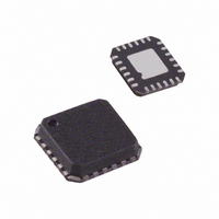
ADA4938-2ACPZ-R2 Analog Devices Inc, ADA4938-2ACPZ-R2 Datasheet - Page 21

ADA4938-2ACPZ-R2
Manufacturer Part Number
ADA4938-2ACPZ-R2
Description
IC ADC DRIVER DUAL DIFF 24LFCSP
Manufacturer
Analog Devices Inc
Type
ADC Driverr
Datasheet
1.ADA4938-1ACPZ-R7.pdf
(28 pages)
Specifications of ADA4938-2ACPZ-R2
Applications
Data Acquisition
Mounting Type
Surface Mount
Package / Case
24-LFCSP
No. Of Amplifiers
2
Input Offset Voltage
4mV
Bandwidth
1GHz
Slew Rate
4700V/µs
Supply Voltage Range
4.5V To 11V
Supply Current
37mA
Amplifier Case Style
LFCSP
No. Of Pins
24
Rohs Compliant
Yes
Lead Free Status / RoHS Status
Lead free / RoHS Compliant
TERMINATING A SINGLE-ENDED INPUT
Using an example with an input source of 2 V, a source
resistance of 50 Ω, and an overall gain of 1 V/V, four simple
steps must be followed to terminate a single-ended input to the
ADA4938-x.
1. The input impedance is calculated using the formula
2. To provide a 50 Ω termination for the source, the Resistor R
3. To compensate for the imbalance of the gain resistors, a correc-
is calculated such that R
tion resistor (R
Gain Resistor R
the source resistance (R
V
2V
R
V
not affect the termination.
R
S
TS
IN
S
V
2V
/2, which would be the case if the amplifier circuit did
S
= R
50Ω
=
R
S
⎛
⎜
⎜
⎜
⎜
⎝
TH
1
50Ω
R
V
2V
−
S
Figure 63. Calculating Thevenin Equivalent
S
50Ω
Figure 62. Adding Termination Resistor R
Figure 61. Single-Ended Input Impedance
= R
2
TS
×
267Ω
R
G
50Ω
S
) is added in series with the inverting Input
R
(
. R
R
IN
61.9Ω
R
|| R
S
G
R
G
R
TS
F
T
+
T
is equal to the Thevenin equivalent of
200Ω
200Ω
V
= 27.4 Ω. Note that V
R
R
61.9Ω
R
R
OCM
S
T
G
G
F
T
||R
)
200Ω
V
200Ω
|| R
R
R
OCM
⎞
⎟
⎟
⎟
⎟
⎠
G
G
T
=
).
IN
⎛
⎜
⎜
⎜
⎜
⎝
= 50 Ω, or R
1
ADA4938
200Ω
200Ω
−
R
R
F
F
2
+V
–V
ADA4938
200Ω
200Ω
1.1V
×
V
R
R
S
S
TH
(200
F
F
+V
–V
200
200
S
S
27.4Ω
R
+
T
TH
TH
200)
= 61.9 Ω.
T
is not equal to
R
⎞
⎟
⎟
⎟
⎟
⎠
L
=
R
267
V
L
O
V
Ω
O
Rev. A | Page 21 of 28
T
4. Finally, the feedback resistor is recalculated to adjust the
SETTING THE OUTPUT COMMON-MODE VOLTAGE
The V
approximately equal to the midsupply point (average value of
the voltages on V+ and V−). Relying on this internal bias results
in an output common-mode voltage that is within about 100 mV of
the expected value.
In cases where more accurate control of the output common-
mode level is required, it is recommended that an external
source or resistor divider (10 kΩ or greater resistors) be used.
It is also possible to connect the V
level (CML) output of an ADC. However, care must be taken to
ensure that the output has sufficient drive capability. The input
impedance of the V
ADA4938-x devices share one reference output, it is recommended
that a buffer be used.
output voltage to the desired level.
a.
b.
R
R
OCM
V
2V
F
F
S
1.1V
V
=
=
Figure 65. Complete Single-Ended-to-Differential System
To make the output voltage V
using
To return the overall gain to 1 V/V (V
should be
TH
pin of the ADA4938-x is internally biased at a voltage
⎛
⎜
⎜
⎝
⎛
⎜
⎜
⎝
50Ω
V
V
R
S
O
O
×
×
27.4Ω
27.4Ω
R
Figure 64. Balancing Gain Resistor R
(
(
R
TH
V
V
R
R
61.9Ω
TS
27.4Ω
TH
TH
G
G
OCM
R
R
+
+
TS
T
200Ω
V
200Ω
R
R
R
R
OCM
pin is approximately 10 kΩ. If multiple
TS
TS
G
G
200Ω
200Ω
V
)
)
R
R
OCM
⎞
⎟
⎟
⎠
⎞
⎟
⎟
⎠
ADA4938-1/ADA4938-2
G
G
=
=
⎛
⎜
⎝
⎛
⎜
⎝
1
2
200Ω
200Ω
ADA4938
×
R
R
×
OCM
F
F
(200
+V
–V
(200
ADA4938
R
R
S
S
1.1
1.1
input to a common-mode
F
F
O
+V
–V
+
+
= 1 V, R
S
S
27.4)
27.4)
G
O
⎞
⎟
⎠
⎞
⎟
⎠
F
=
= V
=
R
is calculated
L
207
414
V
0.97V
R
S
O
L
= 2 V), R
Ω
Ω
V
O
F


