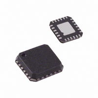
ADA4938-2ACPZ-R2 Analog Devices Inc, ADA4938-2ACPZ-R2 Datasheet - Page 24

ADA4938-2ACPZ-R2
Manufacturer Part Number
ADA4938-2ACPZ-R2
Description
IC ADC DRIVER DUAL DIFF 24LFCSP
Manufacturer
Analog Devices Inc
Type
ADC Driverr
Datasheet
1.ADA4938-1ACPZ-R7.pdf
(28 pages)
Specifications of ADA4938-2ACPZ-R2
Applications
Data Acquisition
Mounting Type
Surface Mount
Package / Case
24-LFCSP
No. Of Amplifiers
2
Input Offset Voltage
4mV
Bandwidth
1GHz
Slew Rate
4700V/µs
Supply Voltage Range
4.5V To 11V
Supply Current
37mA
Amplifier Case Style
LFCSP
No. Of Pins
24
Rohs Compliant
Yes
Lead Free Status / RoHS Status
Lead free / RoHS Compliant
ADA4938-1/ADA4938-2
HIGH PERFORMANCE ADC DRIVING
The ADA4938-x is ideally suited for dc-coupled baseband
applications. The circuit in Figure 69 shows a front-end connection
for an ADA4938-x driving an AD9446, 16-bit, 80 MSPS ADC.
The AD9446 achieves its optimum performance when it is
driven differentially. The ADA4938-x eliminates the need for a
transformer to drive the ADC, performs a single-ended-to-
differential conversion, buffers the driving signal, and provides
appropriate level shifting for dc coupling.
The ADA4938-x is configured with a single 10 V supply and
unity gain for a single-ended input to differential output. The
61.9 Ω termination resistor, in parallel with the single-ended
input impedance of 267 Ω, provides a 50 Ω termination for the
source. The additional 26 Ω (226 Ω total) at the inverting input
balances the parallel impedance of the 50 Ω source and the
termination resistor driving the noninverting input.
The signal generator has a symmetric, ground-referenced bipolar
output. The V
resistor divider to obtain the desired 3.5 V output common-mode.
One-half of the common-mode voltage is fed back to the summing
nodes, biasing −IN and +IN at 1.75 V. For a common-mode vol-
tage of 3.5 V, each ADA4938-x output swings between 2.7 V
and 4.3 V, providing a 3.2 V p-p differential output.
The output of the amplifier is dc-coupled to the ADC through a
second-order, low-pass filter with a −3 dB frequency of 50 MHz.
The filter reduces the noise bandwidth of the amplifier and
isolates the driver outputs from the ADC inputs.
The AD9446 is configured for a 4.0 V p-p full-scale input by
setting R1 = R2 = 1 kΩ between the VREF pin and SENSE pin
in Figure 69.
OCM
pin of the ADA4938-x is biased with an external
SIGNAL
GENERATOR
50Ω
50Ω
V
0.1µF
IN
61.9Ω
10V
76.8Ω
Figure 70. ADA4938 Driving an AD9246, a 14-Bit, 125 MSPS ADC
Figure 69. ADA4938 Driving an AD9446, 16-Bit, 80 MSPS ADC
226Ω
30.1Ω
200Ω
90Ω
90Ω
V
V
OCM
OCM
ADA4938
200Ω
+
200Ω
ADA4938
+
200Ω
200Ω
10V
+5V
–5V
Rev. A | Page 24 of 28
33Ω
33Ω
24.3Ω
24.3Ω
10pF
30nH
30nH
The circuit in Figure 70 shows a simplified front-end connection
for an ADA4938-x driving an AD9246, 14-bit, 125 MSPS ADC.
The AD9246 achieves its optimum performance when it is
driven differentially. The ADA4938-x eliminates the need for a
transformer to drive the ADC, performs a single-ended-to-
differential conversion, buffers the driving signal, and provides
appropriate level shifting for dc coupling.
The ADA4938-x is configured with dual ±5 V supplies and a
gain of ~2 V/V for a single-ended input to differential output.
The 76.8 Ω termination resistor, in parallel with the single-
ended input impedance of 137 Ω, provides a 50 Ω dc termination
for the source. The additional 30.1 Ω (120 Ω total) at the inverting
input balances the parallel dc impedance of the 50 Ω source and
the termination resistor driving the noninverting input.
The signal generator has a symmetric, ground-referenced
bipolar output. The V
the CML pin of the AD9246 to set the output common-mode
level at the appropriate point. A portion of this is fed back to the
summing nodes, biasing −IN and +IN at 0.55 V. For a common-
mode voltage of 0.9 V, each ADA4938 output swings between
0.4 V and 1.4 V, providing a 2 V p-p differential output.
The output is dc-coupled to a single-pole, low-pass filter. The filter
reduces the noise bandwidth of the amplifier and provides some
level of isolation from the switched capacitor inputs of the ADC.
The
SENSE pin to AGND. The inputs of the
1 V by connecting the CML output, as shown in Figure 70.
AD9246
VIN+
VIN–
VIN+
47pF
VIN–
AGND
AVDD
AD9246
is set for a 2 V p-p full-scale input by connecting the
1.8V
BUFFER T/H
CLOCK/
TIMING
SENSE
AVDD2
5V (A)
DRVDD
AGND
CML
3.3V (A)
AVDD1
OCM
SENSE
R1
pin of the ADA4938-x is connected to
3.3V (D)
DRVDD
REF
ADC
D13 TO
D0
AD9446
R2
VREF
16
AD9246
are biased at


