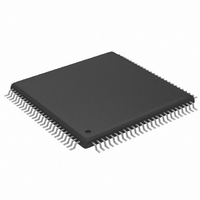
MAX2037CCQ+T Maxim Integrated Products, MAX2037CCQ+T Datasheet - Page 2

MAX2037CCQ+T
Manufacturer Part Number
MAX2037CCQ+T
Description
IC AMP VARIABLE GAIN 100-TQFP
Manufacturer
Maxim Integrated Products
Type
Variable Gain Amplifierr
Datasheet
1.MAX2037CCQT.pdf
(13 pages)
Specifications of MAX2037CCQ+T
Applications
Medical Ultrasound Imaging, Sonar
Mounting Type
Surface Mount
Package / Case
100-TQFP Exposed Pad, 100-eTQFP, 100-HTQFP, 100-VQFP
Lead Free Status / RoHS Status
Lead free / RoHS Compliant
Ultrasound Variable-Gain Amplifier
ABSOLUTE MAXIMUM RATINGS
V
Any Other Pins to GND...............................-0.3V to (V
VGA Differential Input Voltage (VGIN_+ - VGIN_-)...........8.0V
Analog Gain-Control Input Differential Voltage
Continuous Power Dissipation (T
DC ELECTRICAL CHARACTERISTICS
(Figure 2, V
to GND at each of the VGA differential outputs is 60pF, differential capacitance across the VGA outputs is 10pF, R
values are at V
Note 1: Package thermal resistances were obtained using the method described in JEDEC specification JESD51-7, using a four-
Stresses beyond those listed under “Absolute Maximum Ratings” may cause permanent damage to the device. These are stress ratings only, and functional
operation of the device at these or any other conditions beyond those indicated in the operational sections of the specifications is not implied. Exposure to
absolute maximum rating conditions for extended periods may affect device reliability.
2
Supply Voltage Range
V
Range
Total Power Supply Current
V
V
Current Consumption per
Amplifier Channel
Differential Analog Control
Voltage Range
Differential Analog Control
Common-Mode Voltage
Analog Control Input Source/Sink
Current
LOGIC INPUTS
CMOS Input High Voltage
CMOS Input Low Voltage
CC
(VG_CTL+ - VG_CTL-)...................................................8.0V
100-Pin TQFP
(derated 45.5mW/°C above +70°C).........................3636.4mW
CC
CC
REF
, V
_______________________________________________________________________________________
External Reference Voltage
Supply Current
Current
REF
layer board. For detailed information on package thermal considerations, refer to www.maxim-ic.com/thermal-tutorial.
to GND .................................................-0.3V to +5.5V
PARAMETER
CC
CC
= V
= V
REF
REF
= 4.75V to 5.25V, V
= 5V, T
A
A
= +70°C)
= +25°C, unless otherwise noted.) (Note 2)
SYMBOL
V
I
V
I
V
VCC
V
REF
V
REF
CM
CC
CM
IH
IL
= (3/5)V
(Note 3)
Refers to V
current plus V
Refers to V
Minimum gain
Maximum gain
CC
REF
+ 0.3V)
, T
A
P-P
P-P
CC
CC
= 0°C to +70°C, V
REF
supply
supply current
CONDTIONS
current
Operating Temperature Range...............................0°C to +70°C
Junction Temperature ......................................................+150°C
θ
θ
Storage Temperature Range .............................-40°C to +150°C
Lead Temperature (soldering, 10s) .................................+300°C
JC
JA
(Note 1) .....................................................................+2°C/W
(Note 1) ...................................................................+22°C/W
PD = 0
PD = 1
GND
= 0, PD = 0, no RF signals applied, capacitance
MIN
4.75
4.75
2.85
2.0
TYP
204
192
3.0
4.5
27
12
24
+2
-2
5
5
MAX
5.25
5.25
3.15
L
231
216
0.8
33
15
27
5
= 1kΩ. Typical
UNITS
V
mA
mA
mA
mA
mA
P-P
V
V
V
V
V


