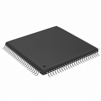
MAX2037CCQ+T Maxim Integrated Products, MAX2037CCQ+T Datasheet - Page 9

MAX2037CCQ+T
Manufacturer Part Number
MAX2037CCQ+T
Description
IC AMP VARIABLE GAIN 100-TQFP
Manufacturer
Maxim Integrated Products
Type
Variable Gain Amplifierr
Datasheet
1.MAX2037CCQT.pdf
(13 pages)
Specifications of MAX2037CCQ+T
Applications
Medical Ultrasound Imaging, Sonar
Mounting Type
Surface Mount
Package / Case
100-TQFP Exposed Pad, 100-eTQFP, 100-HTQFP, 100-VQFP
Lead Free Status / RoHS Status
Lead free / RoHS Compliant
The MAX2037’s VGAs are optimized for high linearity,
high dynamic range, and low output noise perfor-
mance, making this component ideal for ultrasound-
imaging applications. The VGA paths also exhibit a
channel-to-channel crosstalk of -80dB at 10MHz and an
absolute gain error of less than ±0.25dB for minimal
channel-to-channel focusing error in an ultrasound sys-
tem. Each VGA path includes circuitry for adjusting
analog gain, an output buffer with differential output
ports (VGOUT_+, VGOUT_-) for driving ADCs, and dif-
ferential input ports (VGIN_+, VGIN_-) that are ideal for
directly interfacing to the MAX2034 quad LNA. See the
Functional Diagram for details.
The VGA has an adjustable gain range from -12.5dB to
+29.5dB, achieving a total dynamic range of typically
42dB. The VGA gain can be adjusted with the differen-
tial gain-control input VG_CTL+ and VG_CTL-. Set the
differential gain-control input voltage at -2V for maxi-
mum gain and +2V for minimum gain. The differential
analog control common-mode voltage is typically 3.0V.
PIN
100
61
62
63
67
68
70
71
74
75
77
78
86
94
95
99
—
V G_C LAMP _M OD E
_______________________________________________________________________________________
VGOUT4+
VGOUT3+
VGOUT2+
VGOUT1+
VGOUT5-
VG_CTL+
VGOUT4-
VGOUT3-
VGOUT2-
VGOUT1-
VG_CTL-
VGIN1+
VGIN2+
VGIN1-
VGIN2-
NAME
Detailed Description
EP
Ultrasound Variable-Gain Amplifier
VGA Channel 5 Inverting Differential Output
VGA Analog Gain-Control Inverting Input
VGA Analog Gain-Control Noninverting Input
VGA Channel 4 Noninverting Differential Output
VGA Channel 4 Inverting Differential Output
VGA Channel 3 Noninverting Differential Output
VGA Channel 3 Inverting Differential Output
VGA Channel 2 Noninverting Differential Output
VGA Channel 2 Inverting Differential Output
VGA Channel 1 Noninverting Differential Output
VGA Channel 1 Inverting Differential Output
V GA C l am p M od e E nab l e. D r i ve V G _C LAM P _M OD E l ow to enab l e V GA cl am p i ng . V G A outp ut
w i l l b e cl am p ed at typ i cal l y 2.4V
cl am p m od e.
VGA Channel 1 Inverting Differential Input
VGA Channel 1 Noninverting Differential Input
VGA Channel 2 Inverting Differential Input
VGA Channel 2 Noninverting Differential Input
Exposed pad. Internally connected to GND. Solder the exposed pad to the ground plane
using multiple vias.
A clamp is provided to limit the VGA output signals to
avoid overdriving the ADC or to prevent ADC satura-
tion. Set VG_CLAMP_MODE low to clamp the VGA dif-
ferential outputs at 2.4V
high to disable the clamp.
The device can also be powered down with PD. Set PD
to logic-high for power-down mode. In power-down
mode, the device draws a total supply current of 27mA.
Set PD to a logic-low for normal operation
The device is also optimized for quick overload recov-
ery for operation under the large input signal conditions
that are typically found in ultrasound input buffer imag-
ing applications. See the Typical Operating
Characteristics for an illustration of the rapid recovery
time from a transmit-related overload.
P - P
d i ffer enti al . D r i ve V G_C LAM P _M O D E hi g h to d i sab l e V G A
FUNCTION
Pin Description (continued)
P-P
. Set the VG_CLAMP_MODE
Overload Recovery
Power Down
VGA Clamp
9


