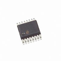
ISL59830IAZ Intersil, ISL59830IAZ Datasheet - Page 11

ISL59830IAZ
Manufacturer Part Number
ISL59830IAZ
Description
IC DRIVER VIDEO SGL 3.3V 16QSOP
Manufacturer
Intersil
Datasheet
1.ISL59830IAZ.pdf
(14 pages)
Specifications of ISL59830IAZ
Applications
Driver
Output Type
Rail-to-Rail
Number Of Circuits
3
-3db Bandwidth
200MHz
Slew Rate
500 V/µs
Current - Supply
120mA
Current - Output / Channel
50mA
Voltage - Supply, Single/dual (±)
3 V ~ 3.6 V
Mounting Type
Surface Mount
Package / Case
16-QSOP
Lead Free Status / RoHS Status
Lead free / RoHS Compliant
Available stocks
Company
Part Number
Manufacturer
Quantity
Price
Part Number:
ISL59830IAZ
Manufacturer:
INTERSIL
Quantity:
20 000
Company:
Part Number:
ISL59830IAZ-T7
Manufacturer:
Intersil
Quantity:
2 400
Part Number:
ISL59830IAZ.
Manufacturer:
INTERSIL
Quantity:
20 000
exponentially modulated by the magnitude of the open loop
gain, output impedance increases with frequency as the
open loop gain decreases with frequency. This inductive-like
effect of the output impedance is countered in the ISL59830
with proprietary output stage topology, keeping the output
impedance low over a wide frequency range and making it
possible to easily and effectively drive relatively heavy
capacitive loads.(See Figure 11).
The Charge Pump
The ISL59830 charge pump provides a bottom rail up to
1.65V below ground while operating on a 0V to 3.3V power
supply. The charge pump is internally regulated to one-half
the potential of the positive supply. This internal multi-phase
charge pump is driven by a 160MHz differential ring
oscillator driving a series of inverters and charge storage
circuitry. Each series inverter charges and places parallel
adjoining charge circuitry slightly out of phase with the
immediately preceding block. The overall effect is sequential
discharge and generation of a very low ripple of about 10mV
that is applied to the amplifiers providing a negative rail of up
to -1.65V.
There are two options to reduce the output supply noise.
• Add a 120Ω bead in series between V
Add a 20pF capacitor between the back load 75Ω resistor
and ground (see the ISL59830A + DC-Restore Solution
schematic on page 10).
further reduce ripple.
BIAS
I
N
+
11
I
N
-
CC
and DV
CC
to
ISL59830
FIGURE 27.
The system operates at sufficiently high frequencies that any
related charge pump noise is far beyond standard video
bandwidth requirements. Still, appropriate bypassing
discipline must be observed, and all pins related to either the
power supply or the charge pump must be properly
bypassed. See "Power Supply Bypassing and Printed Circuit
Board Layout" in this section.
To maximize resistance to latch-up, a diode should be added
between the VEEOUT pin (anode) and GND (cathode), as
shown in the Demo Board Schematic. This prevents VEE
from rising more than 0.7V above ground during startup.
(VEE > 1V above GND can cause latchup under some
conditions.)
FIGURE 28. CHARGE PUMP OSCILLATION (AMP OUTPUT)
TIME (20ns/DIV)
OUT
May 4, 2006
FN7489.6


