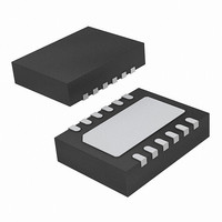
ISL59831IRTZ-T7 Intersil, ISL59831IRTZ-T7 Datasheet - Page 3

ISL59831IRTZ-T7
Manufacturer Part Number
ISL59831IRTZ-T7
Description
IC VIDEO DVR SGL 3.3V 12-TDFN
Manufacturer
Intersil
Datasheet
1.ISL59831IRTZ.pdf
(11 pages)
Specifications of ISL59831IRTZ-T7
Applications
Reconstruction Filter
Number Of Circuits
1
Current - Supply
6mA
Current - Output / Channel
50mA
Voltage - Supply, Single/dual (±)
3 V ~ 3.6 V
Mounting Type
Surface Mount
Package / Case
12-TDFN
Lead Free Status / RoHS Status
Lead free / RoHS Compliant
Absolute Maximum Ratings
V
V
Maximum Continuous Output Current . . . . . . . . . . . . . . . . . . ±50mA
Maximum Current into Any Pin . . . . . . . . . . . . . . . . . . . . . . . ±50mA
ESD Rating
Operating Conditions
Temperature Range . . . . . . . . . . . . . . . . . . . . . . . . . .-40°C to +85°C
CAUTION: Stresses above those listed in “Absolute Maximum Ratings” may cause permanent damage to the device. This is a stress only rating and operation of the
device at these or any other conditions above those indicated in the operational sections of this specification is not implied.
IMPORTANT NOTE: All parameters having Min/Max specifications are guaranteed. Typical values are for information purposes only. Unless otherwise noted, all tests
are at the specified temperature and are pulsed tests, therefore: T
NOTES:
Electrical Specifications
DC CHARACTERISTICS
AC CHARACTERISTICS
V
1. θ
2. θ
VCLAMPIN Input Clamp Level
CC
IN
V
SYMBOL
CLAMPOUT
Human Body Model (Per MIL-STD-883 Method 3015.7) . . .3500V
Machine Model (Per EIAJ ED-4701 Method C-111) . . . . . . . .350V
V
PSRR
CPVEE
I
CC,
CLAMP
IN_MAX
to GND . . . . . . . . . . . . . . . . . . . . . . . GND - 0.3V to V
Tech Brief TB379.
SNR
V
A
A
to GND. . . . . . . . . . . . . . . . . . . . . . . . . . . . . . . . . . . . . . . . . .4V
I
I
I
JA
JC
dG
I
A
dP
CC
CP
PD
IN
OS
PB
SB
V
V
, “case temperature” location is at the center of the exposed metal pad on the package underside. See Tech Brief TB379.
is measured in free air with the component mounted on a high effective thermal conductivity test board with “direct attach” features. See
DC
CP
Supply Range
Charge Pump Output
Supply Current
Charge Pump Supply
Current
Power Down Current
Input Pulldown Current
DC Gain
Max DC Input Range
Output Sync Tip Clamp
Level
Output Level Shift
Clamp Restore Current Force V
Power Supply Rejection VCC = +3.0 to +3.6
Passband Flatness
Stopband Attenuation
Differential Gain
Differential Phase
Signal to Noise Ratio
PARAMETER
3
V
C
CP
IN
(T
A
No load
No load
ENABLE = 0.4V
V
DC-Coupled Input, guaranteed by output linearity
Sync height = 293mV, V
Input floating
Sync height = 293mV, V
DC-coupled input
f = 100kHz to 5MHz relative to 100kHz
f ≥ 27MHz relative to 100kHz
5-step modulated staircase
5-step modulated staircase
Peak signal (1.4V
= 0.1µF ±20%, R
= V
IN
= +25°C)
CC
= 0.5V
= 3.3V, C
IN
= -0.3V
F
L
J
P-P
CC
= 56nF ±20%, C
= 150Ω, C
= T
) to RMS noise, f = 10Hz to 50MHz
+ 0.3V
C
= T
CONDITIONS
IN
IN
ISL59831
A
≤ 0, AC-coupled input
> 0, output shifted relative to input,
L
= 0pF, T
S
= 0.1µF ±20%, R
Thermal Information
Thermal Resistance (Typical, Notes 1, 2) θ
Maximum Junction Temperature (Plastic Package) . . . . . . . +150°C
Maximum Storage Temperature Range . . . . . . . . . .-65°C to +150°C
Maximum Lead Temperature (Soldering 10s) . . . . . . . . . . . . +300°C
Pb-free reflow profile . . . . . . . . . . . . . . . . . . . . . . . . . .see link below
A
4x3 TDFN Package . . . . . . . . . . . . . . .
http://www.intersil.com/pbfree/Pb-FreeReflow.asp
= +27°C, unless otherwise specified.
FIL
= 20Ω ±1%, C
-500
-530
MIN
-1.1
3.0
0.5
1.9
1.4
35
25
4
5
0
2
0
FIL
= 0.22µF ±20%,
-550
-592
TYP
0.35
-1.9
3.3
3.9
0.4
40
50
44
59
6
9
2
2
2
JA
(°C/W)
41
MAX
2.06
-600
-650
-2.4
3.6
8.5
4.5
20
80
5
2
March 29, 2007
θ
JC
FN6266.0
3.5
(°C/W)
UNIT
V/V
mA
mA
mV
mV
mV
mA
µA
µA
dB
dB
dB
dB
%
V
V
V
°


