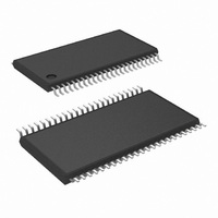
LM8207MTX/NOPB National Semiconductor, LM8207MTX/NOPB Datasheet - Page 19

LM8207MTX/NOPB
Manufacturer Part Number
LM8207MTX/NOPB
Description
IC BUFFER/DVR/VREF 48-TSSOP
Manufacturer
National Semiconductor
Datasheet
1.LM8207MTNOPB.pdf
(22 pages)
Specifications of LM8207MTX/NOPB
Applications
TFT-LCD Panels: Gamma Buffer, VCOM Driver
Output Type
Rail-to-Rail
Number Of Circuits
18
-3db Bandwidth
2MHz
Slew Rate
1 V/µs
Current - Supply
6.5mA
Current - Output / Channel
50mA
Voltage - Supply, Single/dual (±)
6 V ~ 16 V
Mounting Type
Surface Mount
Package / Case
48-TFSOP (0.240", 6.10mm Width)
Lead Free Status / RoHS Status
Lead free / RoHS Compliant
Other names
LM8207MTX
Application Section
MAXIMUM POWER DISSIPATION
The maximum power dissipation in the LM8207 TSSOP
package depends on the ambient temperature and the in-
crease of the junction temperature of the die. Exceeding the
maximum temperature will damage the part. (See the Abso-
lute Maximum Ratings table on page 2 of the datasheet.)
The V
conditions. Driving a continuous current of several hundred
mA to a load will damage the part due to the high power
consumption of the output stage of the V
The maximum operating temperature can be calculated us-
ing this formula:
Where
Example:
The estimated power consumption of the LM8207 in a
steady state situation with no load is:
For an ambient temperature T
power of 100.8 mW, the junction temperature T
This will not exceed the maximum operating temperature.
T
θ
P
V
I
OUT_V
I
V
(V
(16 V – 14.4 V) x 3 mA
Total steady state power
dissipation
DD
LOAD
JA
A
DISSIPATION
DD
DD
DD
x I
COM
- OUT_V
DD
REF
buffer of the LM8207 is designed for use in pulsed
= Ambient temperature
= Thermal resistance of package (See
Operating Ratings table on page 2)
(84˚C/W)
= Total power dissipation of the LM8207
REF
T
J
= T
) x I
A
LOAD
+ θ
JA
=
x P
A
DISSIPATION
= 16V
= 6 mA (all buffers within
normal operating range)
= 14.4V
= 3 mA
= 16 V x 6 mA
= 4.8 mW
= 100.8 mW
of 40˚C and a dissipated
(Continued)
COM
buffer.
J
will be 49˚C.
(3)
19
Two issues are not considered in the calculation:
Example:
When the LM8207 is in steady state biasing, the V buffer is
considered at three various load conditions:
When I
Temperature!
EVALUATION BOARD
For testing purposes an evaluation board is available. It is
intended to evaluate the following functions:
• Continuous power dissipation of the gamma buffers. This
• Pulsed power dissipation of the buffers. The RMS value
• The Voltage Reference is fully adjustable within the op-
• The Gamma correction curve is user defined using exter-
• The V
• For testing, an additional dummy load can be connected
I
is load dependent, and can be calculated using the volt-
age drop over the output stage times the output current:
P = (V
P = (V
of this pulsed current depends on the magnitude of the
current fluctuations and the duty cycle. This can majorly
contribute to the total power dissipation.
OUTRMS
erating range. For optimal output voltage ranges, user
defined resistors can be trimmed by using two resistors in
series.
nal resistors. Each optimal value can be achieved by
using two series resistors for fine-tuning.
National Semiconductor’s LM8342 programmable V
calibrator, or using an external supply.
to all outputs of the gamma buffers.
(mA)
100
10
50
OUTRMS
DD
GMAx
COM
-V
= 100 mA, the package (T
GMAx
) x I
node input voltage can be achieved using
Level (V)
V
COM
OUT
8
8
8
) x I
for current sinking
OUT
Dissipation
for current sourcing
(mW)
400
800
80
J
) will exceed the Operating
Temp
Rise
35
67
7
www.national.com
107
56
83
T
J
COM


