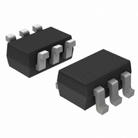
NCS2561SQT1G ON Semiconductor, NCS2561SQT1G Datasheet

NCS2561SQT1G
Specifications of NCS2561SQT1G
Available stocks
Related parts for NCS2561SQT1G
NCS2561SQT1G Summary of contents
Page 1
... Level 2−pole Shifter filter − 2 GND Figure 1. Block Diagram © Semiconductor Components Industries, LLC, 2011 February, 2011 − Rev. 2 NCS2561SQT1G †For information on tape and reel specifications, 5 Related Resource: OUT Refer to Application Note AND8457/D for details 4 regarding SAG Correction SAG 3 1 http://onsemi.com ...
Page 2
PIN FUNCTION AND DESCRIPTION Pin Name Type 1 IN Input Video Input 2 GND Ground Ground 3 SAG Output Sag Compensation 4 OUT Output Video Output 5 Enable Input Enable / Disable Function: High = Enable, Low = Disable. When ...
Page 3
DC ELECTRICAL CHARACTERISTICS with V Symbol Characteristic DC PERFORMANCE V Offset Level−Shift Output Voltage OLS T = −40°C to +125°C (Note Input Bias Current IB V Input Voltage Range (Note Voltage Gain V V ...
Page 4
TYPICAL CHARACTERISTICS Figure 2. Frequency Response Figure 4. Differential Gain Figure 6. PSRR vs. Frequency ( +25°C and R = 150 W, unless otherwise specified Figure 3. Group Delay vs. Frequency Figure 5. Differential Phase Figure ...
Page 5
Figure 8. Quiescent Current vs. Temperature ( Figure 9. Signal−to−Noise Ratio vs. Temperature http://onsemi.com 5 ...
Page 6
The NCS2561 is a single video driver optimized for portable applications with low power consumption in a space saving SC−88 package. It includes sag correction circuitry allowing significant reduction of the AC−coupled output capacitor. Internal Level Shift The input common ...
Page 7
Sag Correction Video drivers that do not incorporate sag compensation traditionally recommend a large coupling capacitor (220 mF) on the output of the video driver. Larger output coupling capacitors (≥ 470 mF) are often chosen by design engineers when the ...
Page 8
The Csag value has no significant impact on the coupling even as the value increases. A value recommended for optimal performance. To achieve similar behavior to an output coupling capacitor value Cout = 220 mF (no ...
Page 9
DC−Coupled Output Having efficient output AC−coupled capability thanks to the sag correction option, with the built−in level shifter, the NCS2561 can also be DC−coupled to a 150 W load. This has the advantage of eliminating the AC−coupling capacitors at the ...
Page 10
Figure 18. Multiburst Test with two 150 W loads ESD Protection All the device pins are protected against electrostatic discharge at a level HBM. The output has been considered with a particular attention with ESD structure able ...
Page 11
... Pb−Free strategy and soldering details, please download the ON Semiconductor Soldering and Mounting Techniques Reference Manual, SOLDERRM/D. ON Semiconductor and are registered trademarks of Semiconductor Components Industries, LLC (SCILLC). SCILLC reserves the right to make changes without further notice to any products herein ...


