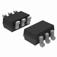
NCS2561SQT1G ON Semiconductor, NCS2561SQT1G Datasheet - Page 3

NCS2561SQT1G
Manufacturer Part Number
NCS2561SQT1G
Description
IC OP AMP HS W/FILTER SC-88
Manufacturer
ON Semiconductor
Datasheet
1.NCS2561SQT1G.pdf
(11 pages)
Specifications of NCS2561SQT1G
Applications
Filter
Number Of Circuits
1
Current - Supply
6mA
Current - Output / Channel
50mA
Voltage - Supply, Single/dual (±)
2.7 V ~ 3.3 V
Mounting Type
Surface Mount
Package / Case
6-TSSOP, SC-88, SOT-363
Lead Free Status / RoHS Status
Lead free / RoHS Compliant
Available stocks
Company
Part Number
Manufacturer
Quantity
Price
Part Number:
NCS2561SQT1G
Manufacturer:
ON/安森美
Quantity:
20 000
3. Guaranteed by design and/or characterization.
4. Limited by output swing and internal gain.
5. Output low voltage level is limited by the internal level shift circuitry.
6. The normalized gain is guaranteed by design and characterization. The max normalized gain of +0.8 dB is the result of smooth peaking
DC ELECTRICAL CHARACTERISTICS with V
AC ELECTRICAL CHARACTERISTICS with V
Symbol
Symbol
DC PERFORMANCE
OUTPUT CHARACTERISTICS
POWER SUPPLY
FREQUENCY DOMAIN PERFORMANCE
TIME DOMAIN RESPONSE
I
PSRR
CC, ON
V
SNR
V
V
t
V
I
DT
(pre−emphasis, see figure 2) taking into account the increase of the losses at the highest frequencies into connectors and cable at the output.
For frequencies lower than 2 MHz the max normalized gain is 0.4 dB.
OFF
V
V
t
V
dG
OFF
A
CC,
An
dP
OLS
I
ON
I
IB
OH
CC
OL
O
IN
IH
V
IL
g
Offset Level−Shift Output Voltage
T
Input Bias Current
Input Voltage Range (Note 4)
Voltage Gain
Enable Input High Level Voltage
Enable Input Low Level Voltage
Output High Level Voltage
Output Low Level Voltage
(Note 5)
Output Current
Operating Voltage Range
Power Supply Current − Enabled
T
Power Supply Current − Disabled
Power Supply Rejection Ratio
Normalized Passband Gain (Note
6)
Differential Gain
Differential Phase
Signal to Noise Ratio
Group Delay Variation
Turn ON Time
Turn OFF Time
A
A
= −40°C to +125°C (Note 3)
= −40°C to +125°C (Note 3)
Characteristic
Characteristic
V
V
V
V
V
V
V
V
CC
CC
CC
CC
IN
IN
CC
CC
CC
CC
V
=3.3 V, f=1.0 MHz , V
=3.3 V, f=4.5 MHz , V
CC
= 0 V, V
= 0 V, V
= 3.3 V, A
= 3.3 V, A
f = 27 MHz, V
f = 3.58 MHz, 4.43 MHz
f = 3.58 MHz, 4.43 MHz
= 3.3 V, 100 kHz to 5.0 MHz
= 2.7 V to 3.3 V
V
= 2.7 V to 3.3 V
= 3.3 V, 100% White Signal
http://onsemi.com
100 IRE White Level
V
CC
R
= 3.3 V, 0 < V
R
CC
L
L
= 150 W to GND
= 3.3 V, V
40 IRE Sync,
V
V
Conditions
= 75 W to GND
Conditions
= 2.7 V to 3.3 V
CC
CC
CC
CC
V
V
= 3.3 V, I
= 3.3 V, I
= 3.3 V
= 3.3 V
= +2, R
= +2, R
3
O
IN
= 2 V
IN
= 0 V
L
L
< 1.5 V
(T
O
O
(T
O
O
= 150 W,
= 150 W,
p−p
A
= 0 mA
= 0 mA
A
=2 V
=2 V
= +25°C, R
= +25°C, R
p−p
p−p
V
L
L
CC
GND
GND
= 150 W to GND, unless otherwise specified)
= 150 W to GND, unless otherwise specified)
−0.4
−0.2
Min
Min
−18
5.8
1.6
2.7
10
− 0.3
V
V
CC
CC
+0.4
Typ
Typ
±50
±80
−22
6.0
6.0
1.5
0.5
1.0
1.5
60
60
±3
60
70
15
50
0
− 0.1
− 0.3
V
CC
Max
Max
+0.4
+0.8
V
6.2
0.8
3.3
7.5
9.0
5.0
80
CC
− 1.5
mV/V
Unit
Unit
mV
mV
mA
mA
pA
dB
mA
dB
dB
ns
ms
ns
%
V
V
V
V
V
°


