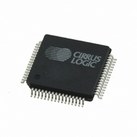
CS44600-CQZ Cirrus Logic Inc, CS44600-CQZ Datasheet - Page 68

CS44600-CQZ
Manufacturer Part Number
CS44600-CQZ
Description
IC AMP CTLR DGTL 6CH 64LQFP
Manufacturer
Cirrus Logic Inc
Type
Digital Amplifier Controllerr
Datasheet
1.CS44600-CQZ.pdf
(76 pages)
Specifications of CS44600-CQZ
Package / Case
64-LQFP
Applications
Automotive Systems
Mounting Type
Surface Mount
Thd Plus Noise
0.05 %
Operating Supply Voltage
2.5 V
Supply Current
150 mA
Maximum Power Dissipation
387 mW
Maximum Operating Temperature
+ 70 C
Mounting Style
SMD/SMT
Minimum Operating Temperature
- 10 C
Supply Type
Digital
Supply Voltage (max)
2.62 V
Supply Voltage (min)
2.37 V
Lead Free Status / RoHS Status
Lead free / RoHS Compliant
For Use With
598-1023 - EVAL BOARD FOR CS44600
Lead Free Status / Rohs Status
Lead free / RoHS Compliant
Other names
598-1068-5
Available stocks
Company
Part Number
Manufacturer
Quantity
Price
Company:
Part Number:
CS44600-CQZ
Manufacturer:
Cirrus Logic Inc
Quantity:
10 000
68
7.31
7.31.1 Differential Signal Delay (DIFF_DLY[2:0])
7.31.2
DIFF_DLY2
7
PWMOUT Delay Register (address 33h)
Power Control (address 02h)” on page 51
will be ignored.
Default = 000
Function:
The Differential Signal Delay bits allow delay adjustment between each channel’s differential signals,
PWMOUTxx+ and PWMOUTxx-. This set of bits control the delay between PWMOUTxx+ and PW-
MOUTxx- across all active channels. The value of this register determines the amount of delay inserted
in the output path. The effective delay is calculated by multiplying the register value by the period of the
PWM_MCLK. This parameter can only be changed when all modulators and associated logic are in the
power-down state by setting the PDN bit in the register
02h)” on page 51
Default = 00000
Function:
The Channel Delay bits allow delay adjustment of each of the PWMOUT differential signal pairs, PW-
MOUTAx+/PWMOUTAx- from the associated PWMOUTBx+/PWMOUTBx-. The value of this register de-
termines the amount of delay inserted in the output path. The effective delay is calculated by multiplying
the register value by the period of the PWM_MCLK. This parameter can only be changed when all mod-
ulators and associated logic are in the power-down state by setting the PDN bit in the register
figuration and Power Control (address 02h)” on page 51
PDN is not set will be ignored.
Channel Delay Settings (CHNL_DLY[4:0])
DIFF_DLY1
6
Binary Code
to a 1b. Attempts to write this register while the PDN is not set will be ignored.
00000
00110
11000
11111
DIFF_DLY0
Table 14. PWM Minimum Pulse Width Settings
5
Table 15. Differential Signal Delay Settings
MIN_PULSE[4:0]
Binary Code
Binary Code
Table 16. Channel Delay Settings
000
001
100
00000
10100
111
00110
11111
Delay Setting(multiply by PWM_MCLK period)
CHNL_DLY4
4
to a 1b. Attempts to write this register while the PDN is not set
Delay Setting (multiply by
PWM_MCLK period)
PWM_MCLK period)
Setting (multiply by
CHNL_DLY3
0 - no delay
Minimum Pulse
0 - no minimum
0 - no delay
3
24
31
“Clock Configuration and Power Control (address
6
to a 1b. Attempts to write this register while the
20
31
6
1
4
7
CHNL_DLY2
2
CHNL_DLY1
1
CS44600
CHNL_DLY0
“Clock Con-
DS633F1
0


