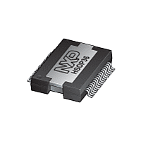
TDA8596 NXP Semiconductors, TDA8596 Datasheet - Page 5

TDA8596
Manufacturer Part Number
TDA8596
Description
The TDA8596 is a quad Bridge Tied Load (BTL) audio power amplifier with symmetricalinputs, made in BCDMOS technology
Manufacturer
NXP Semiconductors
Datasheet
1.TDA8596.pdf
(48 pages)
Available stocks
Company
Part Number
Manufacturer
Quantity
Price
Part Number:
TDA8596TH
Manufacturer:
NXP/恩智浦
Quantity:
20 000
Part Number:
TDA8596TH/N1S
Manufacturer:
NXP/恩智浦
Quantity:
20 000
NXP Semiconductors
7. Functional description
TDA8596_2
Product data sheet
Table 3.
The TDA8596 is a quad BTL audio power amplifier with symmetrical inputs, made in
BCDMOS technology. It contains four independent amplifier channels in BTL configuration
with complementary (PMOST/NMOST) output stages (see
amplifier channel (output offset, connected load, short circuit condition at output pins) can
be read out separately via the I
the supply pins, short circuits at the output pins, overheating and loss-of-ground or
loss-of-V
The temperature pre-warning level and the clip detection levels can be programmed via
the I
or STB) can be programmed. Three different I
connecting a resistor to the ADSEL pin. In case the ADSEL pin is shorted to ground, the
TDA8596 operates in legacy mode. In this mode no I
will change from a two level pin (Standby mode and Operating mode) to a three level pin
(Standby, Mute operating and Normal operating mode).
Symbol
PGND3
OUT3
OUT3+
V
SCL
GAINSEL
OUT4
PGND4
OUT4+
SDA
SVR
ADSEL
STB
OUT2+
PGND2
OUT2
DIAG
V
TAB
P1
P2
2
C-bus. Further, the information that will be available on the diagnostic pins (i.e. DIAG
P
conditions.
Pin description
Pin
16
17
18
19 and 20
21
22
23
24
25
26
27
28
29
30
31
32
33
34 and 35
36
I
2
C-bus controlled 4
Rev. 02 — 8 November 2007
…continued
Description
power ground channel 3
channel 3 negative output
channel 3 positive output
supply voltage 1
I
gain select input (legacy mode only)
channel 4 negative output
power ground channel 4
channel 4 positive output
I
half supply filter capacitor
I
standby (I
programmable second clip indicator
channel 2 positive output
power ground channel 2
channel 2 negative output
diagnostic/clip detection output
supply voltage 2
heatsink connection; must be connected to ground
2
2
2
C-bus clock input
C-bus data input/output
C-bus address select
2
C-bus. The TDA8596 is protected against overvoltage on
2
C-bus mode) or mode pin (legacy mode);
45 W power amplifier with symmetrical inputs
2
C-bus addresses can be selected by
2
C-bus is needed and the STB pin
Figure
1). The status of each
TDA8596
© NXP B.V. 2007. All rights reserved.
5 of 48


