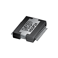
TDF8590TH NXP Semiconductors, TDF8590TH Datasheet - Page 11

TDF8590TH
Manufacturer Part Number
TDF8590TH
Description
The TDF8590TH is a high-efficiency class-D audio power amplifier with low powerdissipation for application in car audio systems
Manufacturer
NXP Semiconductors
Datasheet
1.TDF8590TH.pdf
(30 pages)
Available stocks
Company
Part Number
Manufacturer
Quantity
Price
Part Number:
TDF8590TH
Manufacturer:
NXP/恩智浦
Quantity:
20 000
NXP Semiconductors
Table 5.
In accordance with the Absolute Maximum Rating System (IEC 60134).
[1]
[2]
[3]
8. Thermal characteristics
9. Static characteristics
Table 7.
V
TDF8590TH_2
Product data sheet
Symbol Parameter
V
V
V
V
V
V
V
V
Symbol
Supply
V
I
I
Mode select input; pin MODE (reference to SGND2)
I
V
Diagnostic output; pin DIAG (reference to V
V
V
Audio inputs; pins IN1M, IN1P (reference to SGND1), IN2P and IN2M (reference to SGND2)
V
q(tot)
stb
MODE
P
MODE
OSC
IN1M
IN1P
IN2M
IN2P
DIAG
O
P
MODE
OL
OH
I
= 27 V; f
Pin BOOT should not be loaded by any other means than the boot capacitor. Shorting pin BOOT to V
Pin STABI should not be loaded by an external circuit. Shorting pin STABI to a voltage source or V
Pin DIAG should not be connected to a voltage source or to a pull-up resistor. An example of a circuit that can be used to read out
diagnostic data is given in
voltage on pin MODE
voltage on pin OSC
voltage on pin IN1M
voltage on pin IN1P
voltage on pin IN2M
voltage on pin IN2P
voltage on pin DIAG
output voltage
Limiting values
Static characteristics
osc
Parameter
supply voltage
total quiescent current
standby current
current on pin MODE
voltage on pin mode
LOW-level output voltage
HIGH-level output voltage
input voltage
= 310 kHz; T
Table 6.
Symbol Parameter
R
R
th(j-c)
th(j-a)
Figure
…continued
amb
= 40 C to +85 C; T
7.
thermal resistance from junction to case
thermal resistance from junction to ambient
Thermal characteristics
Conditions
referred to SGND2
referred to V
referred to SGND1
referred to SGND1
referred to SGND2
referred to SGND2
referred to V
Conditions
no load, no filter, no snubber
network connected
T
V
Standby mode
Mute mode
Operating mode
activated OCP or WP
no activated OCP or WP
j
SSD
MODE
= 40 C to +85 C
)
Rev. 02 — 23 April 2007
= 5.5 V
j
= 40 C to +150 C; unless otherwise specified.
2
SSD
SSD
80 W SE (4 ) or 1
[2][3]
[2][3]
[2][3]
[1]
[4]
[4]
[2]
160 W BTL (8 ) class-D amplifier
Conditions
in free air
[3]
Min
-
-
-
0
2.2
4.2
-
-
-
Min
0
0
0
V
14
5
5
5
5
SSP
SS
will damage the device.
SS
0.3
Typ
50
150
100
-
-
-
-
8.4
0
will damage the device.
TDF8590TH
27
Max
8
40
+5
+5
+5
+5
9
V
© NXP B.V. 2007. All rights reserved.
DDP
Typ
1.1
35
Max
65
500
300
0.8
2.8
6
0.8
9
-
29
+ 0.3 V
Unit
V
V
V
V
V
V
V
Unit
K/W
K/W
Unit
V
mA
V
V
V
V
V
V
11 of 30
A
A


