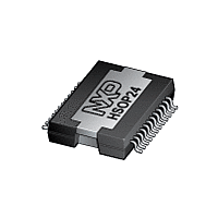
TDF8591TH NXP Semiconductors, TDF8591TH Datasheet - Page 4

TDF8591TH
Manufacturer Part Number
TDF8591TH
Description
The TDF8591TH is a high-efficiency class-D audio power amplifier with low powerdissipation for application in car audio systems
Manufacturer
NXP Semiconductors
Datasheet
1.TDF8591TH.pdf
(34 pages)
Available stocks
Company
Part Number
Manufacturer
Quantity
Price
Part Number:
TDF8591TH
Manufacturer:
NXP/恩智浦
Quantity:
20 000
Company:
Part Number:
TDF8591TH/N1
Manufacturer:
TI
Quantity:
10
Company:
Part Number:
TDF8591TH/N1S
Manufacturer:
XILINX
Quantity:
101
NXP Semiconductors
TDF8591TH_1
Product data sheet
6.2 Mode selection
The TDF8591TH contains two independent amplifier channels with a differential input
stage, high output power, high efficiency (90 %), low distortion and a low quiescent
current. The amplifier channels can be connected in the following configurations:
The TDF8591TH also contains circuits common to both channels such as the oscillator, all
reference sources, the mode functionality and a digital timing manager. For protection a
thermal foldback, temperature, current and voltage protection are built in.
The TDF8591TH can be switched in three operating modes via pin MODE:
The input stage (see
output. To avoid pop noise the DC output offset voltage should be increased gradually at a
mode transition from mute to operating, or vice versa, by limiting the dV
MODE, resulting in a small dV
constant for a gradually increase of the DC output offset voltage between mute and
operating is generated via an RC network on pin MODE. An example of a switching circuit
for driving pin MODE is illustrated in
Table 3.
S1
closed
closed
open
open
Fig 3. Example of mode selection circuit
•
•
•
•
•
Mono Bridge-Tied Load (BTL) amplifier
Dual Single-Ended (SE) amplifiers
Standby mode; the amplifiers are switched off to achieve a very low supply current
Mute mode; the amplifiers are switching idle (50 % duty cycle), but the audio signal at
the output is suppressed by disabling the VI-converter input stages
Operating mode; the amplifiers are fully operational with output signal
Mode selection
Figure
Rev. 01 — 5 March 2008
2
1) contributes to the DC offset measured at the amplifier
V
O(offset)
DDP
100 W SE (4 ) or 1
S2
closed
open
closed
open
5.6 k
5.6 V
/dt for the DC output offset voltage. The required time
Figure 3
S1
5.6 k
and explained in
5.6 k
S2
310 W BTL (4 ) class-D amplifier
001aad836
100 F
(10 V)
MODE
SGND
Mode selection
Standby mode
Standby mode
Mute mode
Operating mode
Table
TDF8591TH
3.
© NXP B.V. 2008. All rights reserved.
MODE
/dt on pin
4 of 34


