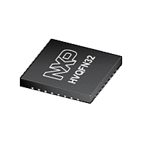
LPC11E11FHN33 NXP Semiconductors, LPC11E11FHN33 Datasheet - Page 12

LPC11E11FHN33
Manufacturer Part Number
LPC11E11FHN33
Description
The LPC11E1x are an ARM Cortex-M0 based, low-cost 32-bit MCU family, designed for 8/16-bit microcontroller applications, offering performance, low power, simple instruction set and memory addressing together with reduced code size compared to existin
Manufacturer
NXP Semiconductors
Datasheet
1.LPC11E11FHN33.pdf
(61 pages)
NXP Semiconductors
Table 3.
[1]
[3]
[4]
[5]
LPC11E1X
Product data sheet
[2]
Symbol
PIO1_23/CT16B1_MAT1/
SSEL1
PIO1_24/CT32B0_MAT0
PIO1_25/CT32B0_MAT1
PIO1_26/CT32B0_MAT2/
RXD
PIO1_27/CT32B0_MAT3/
TXD
PIO1_28/CT32B0_CAP0/
SCLK
PIO1_29/SCK0/
CT32B0_CAP1
PIO1_31
n.c.
n.c.
XTALIN
XTALOUT
V
V
DD
SS
Pin state at reset for default function: I = Input; O = Output; PU = internal pull-up enabled; IA = inactive, no pull-up/down enabled;
F = floating; If the pins are not used, tie floating pins to ground or power to minimize power consumption.
See
reset the chip and wake up from Deep power-down mode. An external pull-up resistor is required on this pin for the Deep power-down
mode.
5 V tolerant pad providing digital I/O functions with configurable pull-up/pull-down resistors and configurable hysteresis (see
I
5 V tolerant pad providing digital I/O functions with configurable pull-up/pull-down resistors and configurable hysteresis (see
includes high-current output driver.
2
C-bus pins compliant with the I
Figure 28
Pin description
for the reset pad configuration. RESET functionality is not available in Deep power-down mode. Use the WAKEUP pin to
13
14
-
-
-
-
-
-
-
-
4
5
6;
29
33
2
18
21
1
11
12
24
31
25
19
20
6
7
8;
44
5;
41
C-bus specification for I
24
27
2
14
15
31
41
-
25
26
8
9
10;
33;
48;
58
7;
54
All information provided in this document is subject to legal disclaimers.
[3]
[3]
[3]
[3]
[3]
[3]
[3]
[3]
[7]
[7]
Reset
state
[1]
I; PU
-
-
I; PU
-
I; PU
-
I; PU
-
-
I; PU
-
-
I; PU
-
-
I; PU
-
-
I; PU
F
F
-
-
-
-
Rev. 1 — 20 February 2012
2
C standard mode, I
Type Description
I/O
O
I/O
I/O
O
I/O
O
I/O
O
I
I/O
O
O
I/O
I
I/O
I/O
I/O
I
I/O
-
-
-
-
-
-
PIO1_23 — General purpose digital input/output pin.
CT16B1_MAT1 — Match output 1 for 16-bit timer 1.
SSEL1 — Slave select for SSP1.
PIO1_24 — General purpose digital input/output pin.
CT32B0_MAT0 — Match output 0 for 32-bit timer 0.
PIO1_25 — General purpose digital input/output pin.
CT32B0_MAT1 — Match output 1 for 32-bit timer 0.
PIO1_26 — General purpose digital input/output pin.
CT32B0_MAT2 — Match output 2 for 32-bit timer 0.
RXD — Receiver input for USART.
PIO1_27 — General purpose digital input/output pin.
CT32B0_MAT3 — Match output 3 for 32-bit timer 0.
TXD — Transmitter output for USART.
PIO1_28 — General purpose digital input/output pin.
CT32B0_CAP0 — Capture input 0 for 32-bit timer 0.
SCLK — Serial clock input/output for USART in
synchronous mode.
PIO1_29 — General purpose digital input/output pin.
SCK0 — Serial clock for SSP0.
CT32B0_CAP1 — Capture input 1 for 32-bit timer 0.
PIO1_31 — General purpose digital input/output pin.
Not connected.
Not connected.
Input to the oscillator circuit and internal clock generator
circuits. Input voltage must not exceed 1.8 V.
Output from the oscillator amplifier.
Supply voltage to the internal regulator, the external rail,
and the ADC. Also used as the ADC reference voltage.
Ground.
2
C Fast-mode, and I
32-bit ARM Cortex-M0 microcontroller
2
C Fast-mode Plus.
LPC11E1x
© NXP B.V. 2012. All rights reserved.
Figure
Figure
12 of 61
27);
27).


