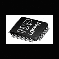
LPC1224FBD64 NXP Semiconductors, LPC1224FBD64 Datasheet - Page 48

LPC1224FBD64
Manufacturer Part Number
LPC1224FBD64
Description
The LPC1224FBD64 is an ARM Cortex-M0 based microcontroller for embedded applications featuring a high level of integration and low power consumption
Manufacturer
NXP Semiconductors
Datasheet
1.LPC1224FBD48.pdf
(61 pages)
Available stocks
Company
Part Number
Manufacturer
Quantity
Price
Company:
Part Number:
LPC1224FBD64/101,1
Manufacturer:
NXP Semiconductors
Quantity:
10 000
Part Number:
LPC1224FBD64/121
Manufacturer:
NXP/恩智浦
Quantity:
20 000
Company:
Part Number:
LPC1224FBD64/121,1
Manufacturer:
NXP Semiconductors
Quantity:
10 000
NXP Semiconductors
Table 16.
T
[1]
[2]
[3]
[4]
[5]
[6]
[7]
[8]
[9]
LPC122X
Product data sheet
Symbol
f
t
t
t
t
t
SCL
f
LOW
HIGH
HD;DAT
SU;DAT
amb
Parameters are valid over operating temperature range unless otherwise specified.
tHD;DAT is the data hold time that is measured from the falling edge of SCL; applies to data in transmission and the acknowledge.
A device must internally provide a hold time of at least 300 ns for the SDA signal (with respect to the V
bridge the undefined region of the falling edge of SCL.
C
The maximum t
250 ns. This allows series protection resistors to be connected in between the SDA and the SCL pins and the SDA/SCL bus lines
without exceeding the maximum specified t
In Fast-mode Plus, fall time is specified the same for both output stage and bus timing. If series resistors are used, designers should
allow for this when considering bus timing.
The maximum t
t
the clock stretches the SCL, the data must be valid by the set-up time before it releases the clock.
tSU;DAT is the data set-up time that is measured with respect to the rising edge of SCL; applies to data in transmission and the
acknowledge.
A Fast-mode I
This will automatically be the case if the device does not stretch the LOW period of the SCL signal. If such a device does stretch the
LOW period of the SCL signal, it must output the next data bit to the SDA line t
Standard-mode I
VD;ACK
=
b
= total capacitance of one bus line in pF. If mixed with Hs-mode devices, faster fall times are allowed.
40
by a transition time. This maximum must only be met if the device does not stretch the LOW period (t
Dynamic characteristic: I
C to +85
11.5 I
2
Parameter
SCL clock frequency
fall time
LOW period of the SCL clock
HIGH period of the SCL clock
data hold time
data set-up time
C-bus device can be used in a Standard-mode I
f
HD;DAT
for the SDA and SCL bus lines is specified at 300 ns. The maximum fall time for the SDA output stage t
2
C-bus specification) before the SCL line is released. Also the acknowledge timing must meet this set-up time.
C.
could be 3.45 s and 0.9 s for Standard-mode and Fast-mode but must be less than the maximum of t
[1]
2
C-bus
2
C-bus pins
All information provided in this document is subject to legal disclaimers.
f
.
Rev. 2 — 26 August 2011
[3][4][5][6]
[2][3][7]
[8][9]
2
C-bus system but the requirement t
Conditions
Standard-mode
Fast-mode
Fast-mode Plus
of both SDA and
SCL signals
Standard-mode
Fast-mode
Fast-mode Plus
Fast-mode
Fast-mode Plus
Standard-mode
Fast-mode
Fast-mode Plus
Standard-mode
Fast-mode
Fast-mode Plus
Standard-mode
Standard-mode
Fast-mode
Fast-mode Plus
r(max)
+ t
32-bit ARM Cortex-M0 microcontroller
SU;DAT
Min
0
0
0
-
20 + 0.1 C
-
4.7
1.3
0.5
4.0
0.6
0.26
0
0
0
250
100
50
= 1000 + 250 = 1250 ns (according to the
SU;DAT
IH
b
(min) of the SCL signal) to
= 250 ns must then be met.
LOW
LPC122x
© NXP B.V. 2011. All rights reserved.
Max
100
1
300
300
120
-
-
-
-
-
-
-
-
-
) of the SCL signal. If
400
-
-
-
f
is specified at
VD;DAT
Unit
kHz
kHz
MHz
ns
ns
ns
s
s
s
s
s
s
s
s
s
ns
ns
ns
48 of 61
or


