MC3302PG ON Semiconductor, MC3302PG Datasheet - Page 2
MC3302PG
Manufacturer Part Number
MC3302PG
Description
IC COMP QUAD SINGLE SUPPLY 14DIP
Manufacturer
ON Semiconductor
Type
General Purposer
Specifications of MC3302PG
Number Of Elements
4
Output Type
CMOS, Open-Collector, TTL
Voltage - Supply
3 V ~ 30 V, ±1.5 V ~ 15 V
Mounting Type
Through Hole
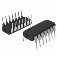
Package / Case
14-DIP (0.300", 7.62mm)
Number Of Channels
4 Channels
Response Time
1.3 us
Offset Voltage (max)
20 mV
Input Bias Current (max)
500 nA
Supply Voltage (max)
30 V
Supply Voltage (min)
3 V
Supply Current (max)
2.5 mA
Maximum Power Dissipation
1000 mW
Maximum Operating Temperature
+ 85 C
Mounting Style
Through Hole
Minimum Operating Temperature
- 40 C
Amplifier Type
Comparator
Current, Input Bias
25 nA
Current, Input Offset
±3 nA
Current, Supply
1 mA
Number Of Amplifiers
Quad
Package Type
SOIC-14
Power Dissipation
1 W
Temperature, Operating, Range
-40 to +85 °C
Voltage, Gain
100 V/mV
Voltage, Input Offset
±3 mVDC
Voltage, Supply
±18 VDC
Comparator Type
General Purpose
No. Of Comparators
4
Ic Output Type
CMOS, TTL
Supply Current
1mA
Supply Voltage Range
3V To 30V
Amplifier Case Style
DIP
No. Of Pins
14
Rohs Compliant
Yes
Output Compatibility
CMOS, TTL
Lead Free Status / RoHS Status
Lead free / RoHS Compliant
Other names
MC3302PGOS
Available stocks
Company
Part Number
Manufacturer
Quantity
Price
Company:

Part Number:
MC3302PG
Manufacturer:
ON
Quantity:
7 700
Company:
Part Number:
MC3302PG
Manufacturer:
ON Semiconductor
Quantity:
4


Stresses exceeding Maximum Ratings may damage the device. Maximum Ratings are stress ratings only. Functional operation above the
Recommended Operating Conditions is not implied. Extended exposure to stresses above the Recommended Operating Conditions may affect
device reliability.
1. The maximum output current may be as high as 20 mA, independent of the magnitude of V
2. V
MAXIMUM RATINGS
Power Supply Voltage
Input Differential Voltage Range
Input Common Mode Voltage Range
Output Short Circuit to Ground (Note 1)
Power Dissipation @ T
Junction Temperature
Operating Ambient Temperature Range
Storage Temperature Range
ESD Protection at any Pin (Note 2)
heating and eventual destruction.
ESD
rating for NCV/SC devices is: Human Body Model − 2000 V; Machine Model − 200 V.
Plastic Package
Derate above 25°C
Human Body Model
Machine Model
A
= 25°C
Rating
V
CC
NOTE: Diagram shown is for 1 comparator.
Figure 1. Circuit Schematic
http://onsemi.com
LM239/LM339/LM2901, V
MC3302
LM239/LM339/LM2901, V
MC3302
LM239
MC3302
LM2901
LM2901V, NCV2901
LM339
+ Input
GND
2
- Input
CC
. Output short circuits to V
Output
Symbol
1/R
V
V
V
V
T
ICMR
I
P
T
T
ESD
SC
IDR
CC
stg
D
A
qJA
J
−40 to +105
−40 to +125
−65 to +150
−0.3 to V
Continuous
+36 or ±18
+30 or ±15
−25 to +85
−40 to +85
0 to +70
Value
1500
150
200
1.0
8.0
36
30
CC
can cause excessive
CC
mW/°C
Unit
Vdc
Vdc
Vdc
°C
°C
°C
W
V
Related parts for MC3302PG
Image
Part Number
Description
Manufacturer
Datasheet
Request
R

Part Number:
Description:
ON Semiconductor [VOLTAGE REGULATOR]
Manufacturer:
ON Semiconductor
Datasheet:
Part Number:
Description:
357-036-542-201 CARDEDGE 36POS DL .156 BLK LOPRO
Manufacturer:
ON Semiconductor
Datasheet:
Part Number:
Description:
357-036-542-201 CARDEDGE 36POS DL .156 BLK LOPRO
Manufacturer:
ON Semiconductor
Datasheet:
Part Number:
Description:
357-036-542-201 CARDEDGE 36POS DL .156 BLK LOPRO
Manufacturer:
ON Semiconductor
Datasheet:
Part Number:
Description:
357-036-542-201 CARDEDGE 36POS DL .156 BLK LOPRO
Manufacturer:
ON Semiconductor
Datasheet:
Part Number:
Description:
357-036-542-201 CARDEDGE 36POS DL .156 BLK LOPRO
Manufacturer:
ON Semiconductor
Datasheet:
Part Number:
Description:
357-036-542-201 CARDEDGE 36POS DL .156 BLK LOPRO
Manufacturer:
ON Semiconductor
Datasheet:
Part Number:
Description:
357-036-542-201 CARDEDGE 36POS DL .156 BLK LOPRO
Manufacturer:
ON Semiconductor
Datasheet:
Part Number:
Description:
357-036-542-201 CARDEDGE 36POS DL .156 BLK LOPRO
Manufacturer:
ON Semiconductor
Datasheet:
Part Number:
Description:
357-036-542-201 CARDEDGE 36POS DL .156 BLK LOPRO
Manufacturer:
ON Semiconductor
Datasheet:
Part Number:
Description:
357-036-542-201 CARDEDGE 36POS DL .156 BLK LOPRO
Manufacturer:
ON Semiconductor
Datasheet:
Part Number:
Description:
Manufacturer:
ON Semiconductor
Datasheet:
Part Number:
Description:
Manufacturer:
ON Semiconductor
Datasheet:
Part Number:
Description:
Manufacturer:
ON Semiconductor
Datasheet: