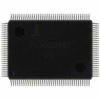
ISL98001CQZ-170 Intersil, ISL98001CQZ-170 Datasheet - Page 27

ISL98001CQZ-170
Manufacturer Part Number
ISL98001CQZ-170
Description
IC TRPL VIDEO DIGITIZER 128-MQFP
Manufacturer
Intersil
Type
Video Digitizerr
Datasheet
1.ISL98001IQZ-140.pdf
(31 pages)
Specifications of ISL98001CQZ-170
Applications
Digital TV, Displays, Digital KVM, Graphics Processing
Mounting Type
Surface Mount
Package / Case
128-MQFP, 128-PQFP
Lead Free Status / RoHS Status
Lead free / RoHS Compliant
Available stocks
Company
Part Number
Manufacturer
Quantity
Price
Company:
Part Number:
ISL98001CQZ-170
Manufacturer:
INTES
Quantity:
274
Part Number:
ISL98001CQZ-170
Manufacturer:
INTERSIL
Quantity:
20 000
To allow input monitoring and mode detection during
power-down, the following blocks remain active:
• Serial interface (including the crystal oscillator) to enable
• Activity and polarity detect functions (registers 0x01 and
• The HSYNC
EMI Considerations
There are two possible sources of EMI on the ISL98001:
Crystal oscillator. The EMI from the crystal oscillator is
negligible. This is due to an amplitude-regulated, low voltage
sine wave oscillator circuit, instead of the typical high-gain
square wave inverter-type oscillator, so there are no harmonics.
Note: The crystal oscillator is not a significant source of EMI.
Digital output switching. This is the largest potential source of
EMI. However, the EMI is determined by the PCB layout and
the loading on the databus. The way to control this is to put
series resistors on the output of all the digital pins (as our demo
board and reference circuits show). These resistors should be
as large as possible, while still meeting the setup and hold
timing requirements of the scaler. We recommend starting with
22Ω. If the databus is heavily loaded (long traces, many other
part on the same bus), this value may need to be reduced. If
the databus is lightly loaded, it may be increased.
Intersil’s recommendations to minimize EMI are:
• Minimize the databus trace length
• Minimize the databus capacitive loading.
If EMI is a problem in the final design, increase the value of the
digital output series resistors to reduce slew rates on the bus.
This can only be done as long as the scaler’s setup and hold
timing requirements continue to be met.
ISL98001 Serial Communication
Overview
The ISL98001 uses a 2-wire serial bus for communication
with its host. SCL is the Serial Clock line, driven by the host,
and SDA is the Serial Data line, which can be driven by all
devices on the bus. SDA is open drain to allow multiple
devices to share the same bus simultaneously.
Communication is accomplished in three steps:
1)
2)
3)
register read/write activity
0x02)
detection)
The Host selects the ISL98001 it wishes to communicate
with.
The Host writes the initial ISL98001 Configuration
Register address it wishes to write to or read from.
The Host writes to or reads from the ISL98001’s
Configuration Register. The ISL98001’s internal address
pointer auto increments, so to read registers 0x00 through
OUT
and VSYNC
27
OUT
pins (for mode
ISL98001
The ISL98001 has a 7-bit address on the serial bus. The
upper 6-bits are permanently set to 100110, with the lower
bit determined by the state of pin 48 (SADDR). This allows
two ISL98001s to be independently controlled while sharing
the same bus.
The bus is nominally inactive, with SDA and SCL high.
Communication begins when the host issues a START
command by taking SDA low while SCL is high (Figure 9).
The ISL98001 continuously monitors the SDA and SCL lines
for the start condition and will not respond to any command
until this condition has been met. The host then transmits the
7-bit serial address plus a R/W bit, indicating if the next
transaction will be a Read (R/W = 1) or a Write (R/W = 0). If
the address transmitted matches that of any device on the
bus, that device must respond with an ACKNOWLEDGE
(Figure 10).
Once the serial address has been transmitted and
acknowledged, one or more bytes of information can be
written to or read from the slave. Communication with the
selected device in the selected direction (read or write) is
ended by a STOP command, where SDA rises while SCL is
high (Figure 9), or a second START command, which is
commonly used to reverse data direction without
relinquishing the bus.
Data on the serial bus must be valid for the entire time SCL
is high (Figure 11). To achieve this, data being written to the
ISL98001 is latched on a delayed version of the rising edge
of SCL. SCL is delayed and deglitched inside the ISL98001
for three crystal clock periods (120ns for a 25MHz crystal) to
eliminate spurious clock pulses that could disrupt serial
communication.
When the contents of the ISL98001 are being read, the SDA
line is updated after the falling edge of SCL, delayed and
deglitched in the same manner.
Configuration Register Write
Figure 12 shows two views of the steps necessary to write
one or more words to the Configuration Register.
Configuration Register Read
Figure 13 shows two views of the steps necessary to read
one or more words from the Configuration Register.
0x1B, for example, one would write 0x00 in step 2, then
repeat step three 28 times, with each read returning the
next register value.
September 21, 2010
FN6148.5


