AD8328ARQ Analog Devices Inc, AD8328ARQ Datasheet - Page 11
AD8328ARQ
Manufacturer Part Number
AD8328ARQ
Description
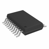
IC LINE DRIVE CABLE 5V 20-QSOP
Manufacturer
Analog Devices Inc
Type
Line Driver, Transmitterr
Datasheet
1.AD8328ARQZ.pdf
(20 pages)
Specifications of AD8328ARQ
Rohs Status
RoHS non-compliant
Applications
Modems, Set-Top Boxes
Mounting Type
Surface Mount
Package / Case
20-QSOP
Available stocks
Company
Part Number
Manufacturer
Quantity
Price

Part Number:
AD8328ARQ
Manufacturer:
ADI/亚德诺
Quantity:
20 000
Company:
Part Number:
AD8328ARQ-REEL
Manufacturer:
QUALCOMM
Quantity:
9 872
Part Number:
AD8328ARQ-REEL
Manufacturer:
ADI/亚德诺
Quantity:
20 000
Part Number:
AD8328ARQZ
Manufacturer:
ADI/亚德诺
Quantity:
20 000


Table 6. Adjacent Channel Power
Channel Symbol Rate (kSym/s)
160
320
640
1280
2560
5120
The output impedance of the AD8328 is 300 Ω, regardless
of whether the amplifier is in transmit enable or transmit
disable mode. This, when combined with a 2:1 voltage ratio
(4:1 impedance ratio) transformer, eliminates the need for
external back termination resistors. If the output signal is being
evaluated using standard 50 Ω test equipment, a minimum loss
75 Ω to 50 Ω pad must be used to provide the test circuit with
the proper impedance match. The AD8328 evaluation board
provides a convenient means to implement a matching attenuator.
Soldering a 43.3 Ω resistor in the R15 placeholder and an 86.6 Ω
resistor in the R16 placeholder allows testing on a 50 Ω system.
When using a matching attenuator, it should be noted that there
is a 5.7 dB of power loss (7.5 dB voltage) through the network.
POWER SUPPLY
The 5 V supply should be delivered to each of the V
low impedance power bus to ensure that each pin is at the same
potential. The power bus should be decoupled to ground using
a 10 μF tantalum capacitor located close to the AD8328. In
addition to the 10 μF capacitor, each V
decoupled to ground with ceramic chip capacitors located close
to the pins. The bypass pin, BYP, should also be decoupled. The
PCB should have a low impedance ground plane covering all
unused portions of the board, except in areas of the board
where input and output traces are in close proximity to the
Z
IN
V
CC
= 150Ω
V
V
DATEN
SDATA
SLEEP
IN+
IN–
TXEN
CLK
10µF
165Ω
1kΩ
1kΩ
1kΩ
1kΩ
1kΩ
CC
pin should be individually
0.1µF
0.1µF
CC
Figure 20. Typical Application Circuit
pins via a
10
1
2
3
4
5
6
7
8
9
GND
V
GND
GND
V
V
GND
DATEN
SDATA
CLK
CC
IN+
IN–
Rev. A | Page 11 of 20
Adjacent Channel Symbol Rate (kSym/s)
160
−58
−58
−60
−62
−64
−66
AD8328
QSOP
SLEEP
RAMP
V
V
TXEN
GND
OUT+
OUT–
GND
BYP
V
NC
320
−60
−59
−58
−60
−62
−65
AD8328 and the output transformer. All AD8328 ground pins
must be connected to the ground plane to ensure proper
grounding of all internal nodes.
SIGNAL INTEGRITY LAYOUT CONSIDERATIONS
Careful attention to printed circuit board layout details will
prevent problems due to board parasitics. Proper RF design
techniques are mandatory. The differential input and output
traces should be kept as short as possible. Keeping the traces
short minimizes parasitic capacitance and inductance. This is
most critical between the outputs of the AD8328 and the 2:1
output transformer. It is also critical that all differential signal
paths be symmetrical in length and width. In addition, the
input and output traces should be adequately spaced to
minimize coupling (crosstalk) through the board. Following
these guidelines optimizes the overall performance of the
AD8328 in all applications.
CC
20
19
18
17
16
15
14
13
12
11
0.1μF
640
−63
−60
−59
−59
−60
−62
0.1μF
0.1μF
1280
−66
−64
−61
−60
−59
−61
TOKO 458PT-1087
TO DIPLEXER
Z
2560
−66
−66
−64
−61
−60
−59
IN
= 75Ω
AD8328
5120
−64
−65
−65
−63
−61
−60
Related parts for AD8328ARQ
Image
Part Number
Description
Manufacturer
Datasheet
Request
R

Part Number:
Description:
±1.7g Dual-Axis IMEMS Accelerometer Evaluation Board
Manufacturer:
Analog Devices Inc
Datasheet:

Part Number:
Description:
Inertial Sensor Evaluation System
Manufacturer:
Analog Devices Inc
Datasheet:
Part Number:
Description:
Manufacturer:
Analog Devices Inc
Datasheet:
Part Number:
Description:
Manufacturer:
Analog Devices Inc
Datasheet:
Part Number:
Description:
Manufacturer:
Analog Devices Inc
Datasheet:
Part Number:
Description:
Manufacturer:
Analog Devices Inc
Datasheet:
Part Number:
Description:
Manufacturer:
Analog Devices Inc
Datasheet:
Part Number:
Description:
Manufacturer:
Analog Devices Inc
Datasheet:
Part Number:
Description:
Manufacturer:
Analog Devices Inc
Datasheet:
Part Number:
Description:
Manufacturer:
Analog Devices Inc
Datasheet:
Part Number:
Description:
Manufacturer:
Analog Devices Inc
Datasheet:
Part Number:
Description:
Manufacturer:
Analog Devices Inc
Datasheet:
Part Number:
Description:
Manufacturer:
Analog Devices Inc
Datasheet: