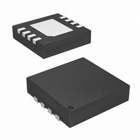
ISL45042AIRZ Intersil, ISL45042AIRZ Datasheet - Page 6

ISL45042AIRZ
Manufacturer Part Number
ISL45042AIRZ
Description
IC LCD CALIBRATOR 8-TDFN
Manufacturer
Intersil
Type
Calibratorr
Datasheet
1.ISL45042AIRZ.pdf
(8 pages)
Specifications of ISL45042AIRZ
Applications
LCD Display
Mounting Type
Surface Mount
Package / Case
8-TDFN
Lead Free Status / RoHS Status
Lead free / RoHS Compliant
Table 1 gives the calculated value of V
values of: R
AV
R
The external R
determines the lowest voltage of the external voltage divider R
and R
V
1.75V. This will keep the output MOS transistor in the saturation
region. Expected current settings and 7-bit accuracy occurs
when the output MOS transistor is operating in the saturation
region. Figure 5 shows the internal connection for the output
MOS transistor. The value of the AV
at the source of the output transistor. This voltage is equal to
(Setting/128) x (AV
to (Setting/128) x (AV
voltage is found using Equation 2. The values of R
Equation 2, should be determined (setting equal to 128) so the
minimum value of V
Power Supply Sequence
The recommendation for power supply sequence would be
to power down the part first (V
programming has occurred, and then power-down the
control power supplies (CTL, CE).
OUT
SET
DD
AVDD
FIGURE 5. OUTPUT CONNECTION CIRCUIT EXAMPLE
TABLE 1. CALCULATED VCOM OUTPUT VOLTAGES
SETTING VALUE
2
pin and I
= 10V.
Resistor
(see Figure 1). The voltage difference between the
100
110
128
SETTING
----------------------------x
10
20
30
40
50
60
70
80
90
SET
1
SET
SET
128
= 24.9kΩ, R
DD
resistor sets the full-scale sink current that
pin (see Figure 5) has to be greater than
OUT
DD
/20). The I
AV DD
----------------- -
20
/20 x R
is greater than 1.75V + AV
1
6
= 200kΩ, R
SET
DD
SET
, AV
). The value of the Drain
DD
VOUT PIN
current is therefore equal
DD
supply sets the voltage
RSET
OUT
VSAT
0.5V
), after 100ms if
V
5.468
5.313
5.141
4.969
4.797
4.625
4.453
4.281
4.109
3.936
3.764
3.592
3.282
2
OUT
for resistors
= 243kΩ, and
AV
1
DD
DD
ISET PIN
and R
R1
R2
= 15V
/20.
2
in
ISL45042A
1
Verifying the Programmed Value
The following sequence can be used to verify the
programmed value without having to sequence the V
supply. To verify the programmed value, follow the following
steps. The ISL45042A will read memory contents and be set
to that value when the CE pin is grounded.
Generating VDD and CE supply from a Larger
Voltage Source
The CE pin has an internal pull-down resistor (see
R
400kΩ to 500kΩ. If your design is using a resistor divider
network to generate the 3.3V supply (for both V
enable programming) from a larger voltage source, the
400kΩ (worst case) resistor needs to be taken into account
as a parallel resistance when the CE pin is connected to this
source. Another design concern is to be able to provide
enough supply current during programming. The ISL45042A
draws about 2mA during this process. Recommended
resistor values are shown in Figure 6. This design will result
in an additional 0.83mA quiescent current flowing through
resistors R
1. Power-up the ISL45042A.
2. CE pin = V
3. Change counter value with CTL pin to desired value.
4. CTL = more than 4.9V and 200ms. Counter value
5. Change the counter value with CTL pin to a different
6. CE pin = Ground.
7. Check that the output value is the one programmed in
INTERNAL
FIGURE 6. APPLICATION GENERATING VDD AND VCE
programmed.
value.
Step 4.
V
CC
VCE
= 5V
A
in Figure 6). The impedance of this resistor is
and R
4kΩ
VOLTAGES
R
2kΩ
R
DD.
B
A
CE
B
.
R
INTERNAL
ISL45042A
= 400kΩ to 500kΩ
SCHMITT
TRIGGER
DD
CE LOGIC
and CE to
July 9, 2008
DD
FN6158.4


