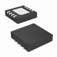
ISL45042AIRZ-TK Intersil, ISL45042AIRZ-TK Datasheet - Page 4

ISL45042AIRZ-TK
Manufacturer Part Number
ISL45042AIRZ-TK
Description
IC LCD CALIBRATOR 8-TDFN
Manufacturer
Intersil
Type
Calibratorr
Datasheet
1.ISL45042AIRZ.pdf
(8 pages)
Specifications of ISL45042AIRZ-TK
Applications
LCD Display
Mounting Type
Surface Mount
Package / Case
8-TDFN
Lead Free Status / RoHS Status
Lead free / RoHS Compliant
Electrical Specifications
NOTES:
CTL EEPROM Programming
Signal Time
Programming Time
SET Voltage Resolution
SET Differential Nonlinearity
SET Zero-Scale Error
SET Full-Scale Error
SET Current
SET External Resistance
AVDD to SET Voltage Attenuation
OUT Settling Time
OUT Voltage Range
OUT Voltage Drift
3. CTL signal only needs to be greater than 4.9V to program EEPROM.
4. Tested at AV
5. The Counter value is set to mid-scale ±4 LSB’s in the Production.
6. Simulated and Determined via Design and NOT Directly Tested.
7. Simulated Maximum Current Draw when Programming EEPROM is 23mA; should be considered when designing Power Supply.
8. A Typical Current of 20µA is Calculated using the AV
9. Parameters with MIN and/or MAX limits are 100% tested at +25°C, unless otherwise specified. Temperature limits established by characterization
and are not production tested.
FIGURE 1. VCOM ADJUSTMENT IN AN LCD PANEL
COLUMN
PARAMETER
DRIVER
CTL
CE
AVDD
SET
ISL45042A
DD
R
SET
= 20V.
+
-
OUT
I
SINK
4
Test Conditions: V
Typicals are at T
SINGLE PIXEL
IN LCD PANEL
AVDD to SET
SYMBOL
SET
SET
OUT
SET
OUT
SET
SET
CTL
AVDD
V
ISET
P
OUT
T
ZSE
FSE
PT
VR
DN
ER
VD
R
ST
R
1
2
A
DD
= +25°C (Continued)
DD
= 3V, AV
VCOM
>4.9V
(Note 5)
Monotonic Over-Temperature
Through R
To GND, AVDD = 20V
To GND, AVDD = 4.5V
to ±0.5 LSB Error Band (Note 6)
(Note 6)
= 10V and R
ISL45042A
TEST CONDITIONS
DD
SET
= 10V, OUT = 5V, R
SET
(Note 8)
= 24.9kΩ. Reference “RSET Resistor” on page 6.
Application Information
The application circuit to adjust the V
panel is shown in Figure 1. The ISL45042A has a 128-step
sink current resolution. The output is connected to an
external voltage divider, that results in decreasing the output
V
CTL Pin
The adjustment of the output V
programming of the non-volatile memory are provided
through a single pin called CTL when the CE pin is high.
The output V
high transition (0.8*V
voltage is decreased with a mid (V
(0.3*V
or maximum value is reached on the 128 steps, the device
will not overflow or underflow beyond that minimum or
maximum value.
Programming of the non-volatile memory occurs when the
CTL pin exceeds 4.9V. The CTL signal needs to remain
above 4.9V for more than 200µs. The level and timing
COM
DD
voltage as you increase the ISL45042A sink current.
SET
) on the CTL pin (see Figure 7). Once the minimum
= 24.9kΩ; Unless Otherwise Specified.
COM
25 to 55
TEMP
(°C)
Full
Full
Full
Full
Full
Full
Full
Full
Full
Full
Full
Full
voltage is increased with a mid (V
DD
VSET + 0.5V
) on the CTL pin. The output V
(Note 9)
MIN
2.25
200
10
7
-
-
-
-
-
-
-
-
COM
DD
voltage and the
COM
/2) to low transition
TYP
1:20
<10
20
20
7
-
-
-
-
-
-
-
-
voltage in an LCD
(Note 9) UNITS
MAX
100
200
±1
±2
±8
45
13
7
-
-
-
-
-
DD
July 9, 2008
FN6158.4
COM
/2) to
LSB
LSB
LSB
Bits
V/V
mV
ms
µA
kΩ
kΩ
µs
µs
V


