AP4955GM Advanced Power Electronics Corp., AP4955GM Datasheet - Page 2
AP4955GM
Manufacturer Part Number
AP4955GM
Description
Advanced Power MOSFETs from APEC provide the designer with the best combination of fast switching,ruggedized device design, lower on-resistance and cost-effectiveness
Manufacturer
Advanced Power Electronics Corp.
Datasheet
1.AP4955GM.pdf
(4 pages)
Specifications of AP4955GM
Vds
-20V
Vgs
±12V
Rds(on) / Max(m?) Vgs@4.5v
45
Rds(on) / Max(m?) Vgs@2.5v
65
Qg (nc)
19
Qgs (nc)
3
Qgd (nc)
6
Id(a)
-5.6
Pd(w)
2
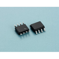
Configuration
Dual P
Package
SO-8
Available stocks
Company
Part Number
Manufacturer
Quantity
Price

Part Number:
AP4955GM
Manufacturer:
APEC/富鼎
Quantity:
20 000
Part Number:
AP4955GM-HF
Manufacturer:
APEC/富鼎
Quantity:
20 000


BV
∆BV
R
V
g
I
I
Q
Q
Q
t
t
t
t
C
C
C
V
t
Q
1.Pulse width limited by Max. junction temperature.
2.Pulse test
3.Surface mounted on 1 in
THIS PRODUCT IS SENSITIVE TO ELECTROSTATIC DISCHARGE, PLEASE HANDLE WITH CAUTION.
USE OF THIS PRODUCT AS A CRITICAL COMPONENT IN LIFE SUPPORT OR OTHER SIMILAR SYSTEMS IS NOT AUTHORIZED.
APEC DOES NOT ASSUME ANY LIABILITY ARISING OUT OF THE APPLICATION OR USE OF ANY PRODUCT OR CIRCUIT DESCRIBED
HEREIN; NEITHER DOES IT CONVEY ANY LICENSE UNDER ITS PATENT RIGHTS, NOR THE RIGHTS OF OTHERS.
APEC RESERVES THE RIGHT TO MAKE CHANGES WITHOUT FURTHER NOTICE TO ANY PRODUCTS HEREIN TO IMPROVE
RELIABILITY, FUNCTION OR DESIGN.
Electrical Characteristics@T
Source-Drain Diode
Notes:
AP4955GM
DSS
GSS
d(on)
r
d(off)
f
rr
fs
GS(th)
SD
DS(ON)
iss
oss
rss
g
gs
gd
rr
DSS
Symbol
Symbol
DSS
/∆T
j
Drain-Source Breakdown Voltage
Breakdown Voltage Temperature Coefficient
Static Drain-Source On-Resistance
Gate Threshold Voltage
Forward Transconductance
Drain-Source Leakage Current
Drain-Source Leakage Current (T
Gate-Source Leakage
Total Gate Charge
Gate-Source Charge
Gate-Drain ("Miller") Charge
Turn-on Delay Time
Rise Time
Turn-off Delay Time
Fall Time
Input Capacitance
Output Capacitance
Reverse Transfer Capacitance
Forward On Voltage
Reverse Recovery Time
Reverse Recovery Charge
2
copper pad of FR4 board ; 135 ℃/W when mounted on min. copper pad.
Parameter
Parameter
2
2
2
2
j
=25
j
=70
o
C(unless otherwise specified)
2
o
C)
V
Reference to 25℃, I
V
V
V
V
V
V
V
I
V
V
V
I
R
R
V
V
f=1.0MHz
I
I
dI/dt=100A/µs
D
D
S
S
GS
GS
GS
DS
DS
DS
DS
GS
DS
GS
DS
GS
DS
=-5A
=-1A
G
D
=-1.6A, V
=-5A,
=10Ω
=3.3Ω,V
=V
=-5V, I
=-20V, V
=-16V, V
=-16V
=-10V
=-20V
=0V, I
=-4.5V, I
=-2.5V, I
=+12V, V
=-4.5V
=0V
GS
V
Test Conditions
Test Conditions
, I
GS
D
D
D
=-250uA
GS
GS
=-5A
=-250uA
=0
D
D
GS
GS
DS
=-5A
=-4A
=-10V
=0V
V
=0V
=0V
=0V
,
D
=-1mA
Min.
Min.
-0.5
-20
-
-
-
-
-
-
-
-
-
-
-
-
-
-
-
-
-
-
-
-
1400 2240
-0.01
Typ.
Typ.
270
230
19
10
52
24
32
22
9
3
6
9
-
-
-
-
-
-
-
-
+100
Max. Units
Max. Units
-1.2
-1.2
-25
45
65
30
-1
-
-
-
-
-
-
-
-
-
-
-
-
-
V/℃
mΩ
mΩ
nC
nC
nC
nC
uA
uA
nA
pF
pF
pF
ns
ns
ns
ns
ns
V
V
S
V
2
Related parts for AP4955GM
Image
Part Number
Description
Manufacturer
Datasheet
Request
R
