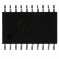
74ABT541CSC Fairchild Semiconductor, 74ABT541CSC Datasheet - Page 2

74ABT541CSC
Manufacturer Part Number
74ABT541CSC
Description
IC BUFF/DVR TRI-ST 8BIT 20SOIC
Manufacturer
Fairchild Semiconductor
Series
74ABTr
Datasheet
1.74ABT541CSC.pdf
(12 pages)
Specifications of 74ABT541CSC
Logic Type
Buffer/Line Driver, Non-Inverting
Number Of Elements
1
Number Of Bits Per Element
8
Current - Output High, Low
32mA, 64mA
Voltage - Supply
4.5 V ~ 5.5 V
Operating Temperature
-40°C ~ 85°C
Mounting Type
Surface Mount
Package / Case
20-SOIC (7.5mm Width)
Logic Family
ABT
Number Of Channels Per Chip
8
Polarity
Non-Inverting
Supply Voltage (max)
5.5 V
Supply Voltage (min)
4.5 V
Maximum Operating Temperature
+ 85 C
Mounting Style
SMD/SMT
High Level Output Current
- 32 mA
Low Level Output Current
64 mA
Minimum Operating Temperature
- 40 C
Number Of Lines (input / Output)
8 / 3
Output Type
3-State
Propagation Delay Time
3.6 ns at 5 V
Dc
0112
Lead Free Status / RoHS Status
Lead free / RoHS Compliant
©1992 Fairchild Semiconductor Corporation
74ABT541 Rev. 1.4
Truth Table
H = HIGH Voltage Level
L = LOW Voltage Level
X = Immaterial
Absolute Maximum Ratings
Stresses exceeding the absolute maximum ratings may damage the device. The device may not function or be
operable above the recommended operating conditions and stressing the parts to these levels is not recommended.
In addition, extended exposure to stresses above the recommended operating conditions may affect device reliability.
The absolute maximum ratings are stress ratings only.
Note:
1. Either voltage limit or current limit is sufficient to protect inputs.
Recommended Operating Conditions
The Recommended Operating Conditions table defines the conditions for actual device operation. Recommended
operating conditions are specified to ensure optimal performance to the datasheet specifications. Fairchild does not
recommend exceeding them or designing to absolute maximum ratings.
Z = High Impedance
Symbol
OE
Symbol
∆ V / ∆ t
H
X
L
L
T
V
V
V
V
STG
T
I
T
T
1
IN
CC
CC
IN
A
O
J
A
Inputs
OE
X
H
L
L
Storage Temperature
Ambient Temperature Under Bias
Junction Temperature Under Bias
V
Input Voltage
Input Current
Voltage Applied to Any Output
Current Applied to Output in LOW State (Max.)
DC Latchup Source Current
Over Voltage Latchup (I/O)
Free Air Ambient Temperature
Supply Voltage
Minimum Input Edge Rate
CC
2
Disabled or Power-Off State
HIGH State
Data Input
Enable Input
Pin Potential to Ground Pin
H
X
X
L
I
(1)
(1)
Outputs
H
Z
Z
L
Parameter
Parameter
2
twice the rated I
Rating
–30mA to +5.0mA
Rating
–65°C to +150°C
–55°C to +125°C
–55°C to +150°C
–40°C to +85°C
+4.5V to +5.5V
–0.5V to +7.0V
–0.5V to +7.0V
–0.5V to 5.5V
www.fairchildsemi.com
–0.5V to V
50mV/ns
20mV/ns
–500mA
OL
(mA)
10V
CC


