MM74C244N Fairchild Semiconductor, MM74C244N Datasheet - Page 3
MM74C244N
Manufacturer Part Number
MM74C244N
Description
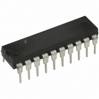
IC BUFF/DVR TRI-ST DUAL 20DIP
Manufacturer
Fairchild Semiconductor
Series
74Cr
Datasheet
1.MM74C244N.pdf
(8 pages)
Specifications of MM74C244N
Logic Type
Buffer/Line Driver, Non-Inverting
Number Of Elements
2
Number Of Bits Per Element
4
Current - Output High, Low
70mA, 70mA
Voltage - Supply
3 V ~ 15 V
Operating Temperature
-55°C ~ 125°C
Mounting Type
Through Hole
Package / Case
20-DIP (0.300", 7.62mm)
Logic Family
74C
Number Of Channels Per Chip
Octal
Polarity
Non-Inverting
Supply Voltage (max)
15 V
Supply Voltage (min)
3 V
Maximum Operating Temperature
125 C
Mounting Style
Through Hole
High Level Output Current
- 2.2 mA
Low Level Output Current
2.2 mA
Maximum Power Dissipation
700 mW
Minimum Operating Temperature
- 55 C
Number Of Lines (input / Output)
1
Output Type
3-State
Propagation Delay Time
90 ns @ 5 V or 70 ns @ 10 V
Lead Free Status / RoHS Status
Lead free / RoHS Compliant
Other names
74C244
74C244N
74C244N
Available stocks
Company
Part Number
Manufacturer
Quantity
Price

Company:
Part Number:
MM74C244N
Manufacturer:
NEC
Quantity:
16 807


CMOS TO CMOS
V
V
V
V
I
I
I
I
CMOS/LPTTL INTERFACE
V
V
V
V
OUTPUT DRIVE (See Family Characteristics Data Sheet) (Short Circuit Current)
I
I
OZ
IN(1)
IN(0)
CC
SOURCE
SINK
Absolute Maximum Ratings
DC Electrical Characteristics
Min/Max limits apply across temperature range, unless otherwise noted
Voltage at Any Pin
Operating Temperature Range
Storage Temperature Range
Power Dissipation
Operating V
Absolute Maximum V
IN(1)
IN(0)
OUT(1)
OUT(0)
IN(1)
IN(0)
OUT(1)
OUT(0)
Symbol
Lead Temperature
Dual-In-Line
Small Outline
(Soldering, 10 seconds)
Logical “1” Input Voltage
Logical “0” Input Voltage
Logical “1” Output Voltage
Logical “0” Output Voltage
3-STATE Output Current
Logical “1” Input Current
Logical “0” Input Current
Supply Current
Logical “1” Input Voltage
Logical “0” Input Voltage
Logical “1” Output Voltage
Logical “0” Output Voltage
Output Source Current
(P-Channel)
Output Sink Current
(N-Channel)
CC
Range
CC
Parameter
0.3V to V
55 C to 125 C
65 C to 150 C
V
V
V
V
V
V
V
V
V
V
V
V
V
V
V
V
V
V
T
V
T
V
T
V
T
(Note 1)
A
A
A
A
CC
CC
CC
CC
CC
CC
CC
CC
CC
CC
CC
CC
CC
CC
CC
CC
CC
CC
CC
CC
CC
25 C
25 C
25 C
25 C
3V to 15V
CC
5V
10V
5V
10V
5V, I
10V, I
5V, I
10V, I
10V, OD
15V, V
15V, V
15V
4.75V
4.75V
4.75V, I
4.75V, I
4.75V, I
5V, V
10V, V
5V, V
10V, V
700 mW
500 mW
260 C
O
O
0.3V
18V
O
O
OUT
OUT
IN
IN
OUT
OUT
Conditions
O
O
O
10 A
10 A
10 A
10 A
15V
0V
V
2.2 mA
3
0V
V
IH
450 A
2.2 mA
0V
V
CC
Note 1: “Absolute Maximum Ratings” are those values beyond which the
safety of the device cannot be guaranteed. Except for “Operating Range”
they are not meant to imply that the devices should be operated at these
limits. The Electrical Characteristics table provides conditions for actual
device operation.
CC
V
V
CC
CC
Min
3.5
8.0
4.5
9.0
2.4
12
48
1.0
14
36
1.5
0.4
0.005
0.005
0.05
Typ
20
70
30
70
www.fairchildsemi.com
Max
300
1.5
2.0
0.5
1.0
1.0
0.8
0.4
10
Units
mA
mA
mA
mA
V
V
V
V
V
V
V
V
V
A
A
A
A
Related parts for MM74C244N
Image
Part Number
Description
Manufacturer
Datasheet
Request
R

Part Number:
Description:
Fairchild Semiconductor [IGBT MODULE]
Manufacturer:
Fairchild Semiconductor
Datasheet:

Part Number:
Description:
Discrete Semiconductor Modules
Manufacturer:
Fairchild Semiconductor
Part Number:
Description:
Discrete Semiconductor Modules
Manufacturer:
Fairchild Semiconductor
Part Number:
Description:
This N-Channel MOSFET is produced using Fairchild Semiconductor’s advanced Power Trench® process
Manufacturer:
Fairchild Semiconductor
Datasheet:
Part Number:
Description:
This N-Channel MOSFET is produced using Fairchild Semiconductor’s advanced Power Trench® process
Manufacturer:
Fairchild Semiconductor
Datasheet:
Part Number:
Description:
This N-Channel MOSFET is produced using Fairchild Semiconductor’s advanced PowerTrench® process
Manufacturer:
Fairchild Semiconductor
Datasheet:
Part Number:
Description:
This N-Channel MOSFET is produced using Fairchild Semiconductor’s advanced PowerTrench® process
Manufacturer:
Fairchild Semiconductor
Datasheet:
Part Number:
Description:
This N-Channel MOSFET is produced using Fairchild Semiconductor’s advanced Power Trench® process
Manufacturer:
Fairchild Semiconductor
Datasheet:
Part Number:
Description:
This N-Channel logic Level MOSFETs are produced using Fairchild Semiconductor‘s advanced Power Trench® process that has been special tailored to minimize the on-state resistance and yet maintain superior switching performance
Manufacturer:
Fairchild Semiconductor
Datasheet:
Part Number:
Description:
This N-Channel MOSFET is produced using Fairchild Semiconductor’s advanced Power Trench® process
Manufacturer:
Fairchild Semiconductor
Datasheet:
Part Number:
Description:
This N-Channel SyncFET™ is produced using Fairchild Semiconductor’s advanced PowerTrench® process
Manufacturer:
Fairchild Semiconductor
Datasheet:
Part Number:
Description:
This N-Channel SyncFET™ is produced using Fairchild Semiconductor’s advanced PowerTrench® process
Manufacturer:
Fairchild Semiconductor
Datasheet:
Part Number:
Description:
This N-Channel SyncFET™ is produced using Fairchild Semiconductor’s advanced PowerTrench® process
Manufacturer:
Fairchild Semiconductor
Datasheet:
Part Number:
Description:
This N-Channel logic Level MOSFETs are produced using Fairchild Semiconductor‘s advanced Power Trench® process that has been special tailored to minimize the on-state resistance and yet maintain superior switching performance
Manufacturer:
Fairchild Semiconductor
Datasheet:
Part Number:
Description:
This N-Channel MOSFET is produced using Fairchild Semiconductor’s advanced Power Trench® process that has been especially tailored to minimize the on-state resistance and yet maintain superior switching performance
Manufacturer:
Fairchild Semiconductor
Datasheet: