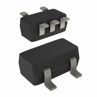
74HC1G125GW,125 NXP Semiconductors, 74HC1G125GW,125 Datasheet - Page 10

74HC1G125GW,125
Manufacturer Part Number
74HC1G125GW,125
Description
IC BUS BUFF DVR TRI-ST 5TSSOP
Manufacturer
NXP Semiconductors
Series
74HCr
Datasheet
1.74HC1G125GW125.pdf
(16 pages)
Specifications of 74HC1G125GW,125
Logic Type
Buffer/Line Driver, Non-Inverting
Package / Case
SC-70-5, SC-88A, SOT-323-5, SOT-353, 5-TSSOP
Number Of Elements
1
Number Of Bits Per Element
1
Current - Output High, Low
7.8mA, 7.8mA
Voltage - Supply
2 V ~ 6 V
Operating Temperature
-40°C ~ 125°C
Mounting Type
Surface Mount
Logic Family
74HC
Number Of Channels Per Chip
1
Polarity
Non-Inverting
Supply Voltage (max)
6 V
Supply Voltage (min)
2 V
Maximum Operating Temperature
125 C
Mounting Style
SMD/SMT
High Level Output Current
- 7.8 mA
Input Bias Current (max)
20 uA
Low Level Output Current
7.8 mA
Maximum Power Dissipation
200 mW
Minimum Operating Temperature
- 40 C
Number Of Lines (input / Output)
2 / 1
Output Type
3-State
Propagation Delay Time
9 ns
Logical Function
Buffer/Line Driver
Number Of Elements
1
Number Of Channels
1
Number Of Inputs
1
Number Of Outputs
1
Operating Supply Voltage (typ)
5V
Package Type
TSSOP
Operating Supply Voltage (max)
6V
Operating Supply Voltage (min)
2V
Quiescent Current
20uA
Technology
CMOS
Pin Count
5
Mounting
Surface Mount
Operating Temp Range
-40C to 125C
Operating Temperature Classification
Automotive
Lead Free Status / RoHS Status
Lead free / RoHS Compliant
Lead Free Status / RoHS Status
Lead free / RoHS Compliant, Lead free / RoHS Compliant
Other names
568-2640-2
935245690125
935245690125
Philips Semiconductors
13. Waveforms
74HC_HCT1G125_5
Product data sheet
Table 12:
Type
74HC1G125
74HCT1G125
Fig 6. Propagation delay data input (A) to output (Y)
Fig 7. Enable and disable times
Measurement points are given in
Measurement points are given in
Logic levels: V
Measurement points
HIGH-to-OFF
OFF-to-HIGH
OFF-to-LOW
LOW-to-OFF
output
OE input
output
OL
Rev. 05 — 23 December 2005
Y output
and V
A input
Input
V
0.5V
1.3 V
GND
GND
V
V
V
M
OH
CC
OL
V
OH
I
CC
GND
are typical output voltage drop that occur with the output load.
V
I
74HC1G125; 74HCT1G125
V
Table
Table
M
enabled
outputs
Output
V
0.5V
1.3 V
t
PLZ
t
PHZ
M
12.
12.
V
CC
M
V
V
M
t
PHL
X
V
Y
V
V
V
X
OL
OL
disabled
outputs
0.3 V
0.3 V
Bus buffer/line driver; 3-state
© Koninklijke Philips Electronics N.V. 2005. All rights reserved.
001aad070
t
PZL
t
t
PZH
PLH
V
M
V
M
outputs
enabled
V
V
V
mna644
Y
OH
OH
0.3 V
0.3 V
10 of 16


