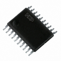
74LVT241PW,112 NXP Semiconductors, 74LVT241PW,112 Datasheet - Page 4

74LVT241PW,112
Manufacturer Part Number
74LVT241PW,112
Description
IC BUFF/DVR TRI-ST DUAL 20TSSOP
Manufacturer
NXP Semiconductors
Series
74LVTr
Datasheet
1.74LVT241PW118.pdf
(16 pages)
Specifications of 74LVT241PW,112
Logic Type
Buffer/Line Driver, Non-Inverting
Number Of Elements
2
Number Of Bits Per Element
4
Current - Output High, Low
32mA, 64mA
Voltage - Supply
2.7 V ~ 3.6 V
Operating Temperature
-40°C ~ 85°C
Mounting Type
Surface Mount
Package / Case
20-TSSOP
Lead Free Status / RoHS Status
Lead free / RoHS Compliant
Other names
74LVT241PW
74LVT241PW
935210110112
74LVT241PW
935210110112
NXP Semiconductors
6. Functional description
Table 3.
[1]
7. Limiting values
Table 4.
In accordance with the Absolute Maximum Rating System (IEC 60134). Voltages are referenced to GND (ground = 0 V).
[1]
[2]
[3]
8. Recommended operating conditions
Table 5.
74LVT241_3
Product data sheet
Inputs
1OE
L
L
H
Symbol
V
V
V
I
I
I
T
T
P
Symbol
V
V
I
IK
OK
O
OH
stg
j
CC
I
O
tot
CC
I
H = HIGH voltage level;
L = LOW voltage level;
X = Don’t care;
Z = High impedance “OFF” state.
The performance capability of a high-performance integrated circuit in conjunction with its thermal environment can create junction
temperatures which are detrimental to reliability. The maximum junction temperature of this integrated circuit should not exceed 150 C.
The input and output negative voltage ratings may be exceeded if the input and output clamp current ratings are observed.
For SO20 packages: above 70 C derate linearly with 8 mW/K.
For SSOP20 and TSSOP20 packages: above 60 C derate linearly with 5.5 mW/K.
For DHVQFN20 packages: above 60 C derate linearly with 4.5 mW/K.
Parameter
supply voltage
input voltage
HIGH-level output current
Function table
Limiting values
Recommended operating conditions
Parameter
supply voltage
input voltage
output voltage
input clamping current
output clamping current
output current
storage temperature
junction temperature
total power dissipation
2OE
H
H
L
1An
L
H
X
Conditions
Conditions
output in OFF or HIGH state
V
V
output in LOW state
output in HIGH state
T
amb
I
O
< 0 V
< 0 V
= 40 C to +85 C
Rev. 03 — 7 May 2008
2An
L
H
X
3.3 V octal buffer/line driver; 3-state
Outputs
1Yn
L
H
Z
[2]
[2]
[3]
Min
-
-
-
0.5
0.5
0.5
50
50
64
65
Min
2.7
0
32
Max
+4.6
+7.0
+7.0
-
-
128
-
+150
+150
500
74LVT241
Max
3.6
5.5
-
© NXP B.V. 2008. All rights reserved.
2Yn
L
H
Z
Unit
V
V
V
mA
mA
mA
mA
mW
C
C
Unit
V
V
mA
4 of 16
[1]


