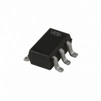
74AUP2G07GW,125 NXP Semiconductors, 74AUP2G07GW,125 Datasheet - Page 12

74AUP2G07GW,125
Manufacturer Part Number
74AUP2G07GW,125
Description
IC BUFF DL LOW PWR OP/DR SC88
Manufacturer
NXP Semiconductors
Series
74AUPr
Datasheet
1.74AUP2G07GW125.pdf
(18 pages)
Specifications of 74AUP2G07GW,125
Package / Case
SC-70-6, SC-88, SOT-363
Logic Type
Buffer/Line Driver, Non-Inverting with Open Drain
Number Of Elements
2
Number Of Bits Per Element
1
Current - Output High, Low
4mA, 4mA
Voltage - Supply
0.8 V ~ 3.6 V
Operating Temperature
-40°C ~ 125°C
Mounting Type
Surface Mount
Logic Family
AUP
Number Of Channels Per Chip
2
Polarity
Non-Inverting
Supply Voltage (max)
3.6 V
Supply Voltage (min)
0.8 V
Maximum Operating Temperature
+ 125 C
Mounting Style
SMD/SMT
Low Level Output Current
4 mA
Minimum Operating Temperature
- 40 C
Output Type
Open Drain
Propagation Delay Time
15.6 ns @ 1.1 V to 1.3 V or 9.7 ns @ 1.65 V to 1.95 V or 9.4 ns @ 1.4 V to 1.6 V or 6.7 ns @ 2.3 V to 2.7 V
Number Of Lines (input / Output)
2 / 2
Lead Free Status / RoHS Status
Lead free / RoHS Compliant
Lead Free Status / RoHS Status
Lead free / RoHS Compliant, Lead free / RoHS Compliant
Other names
568-2577-2
935279985125
935279985125
NXP Semiconductors
Fig 11. Package outline SOT891 (XSON6)
74AUP2G07
Product data sheet
XSON6: plastic extremely thin small outline package; no leads; 6 terminals; body 1 x 1 x 0.5 mm
DIMENSIONS (mm are the original dimensions)
Note
1. Can be visible in some manufacturing processes.
UNIT
mm
VERSION
OUTLINE
SOT891
max
0.5
A
max
0.04
A
1
0.20
0.12
e
b
terminal 1
index area
6×
IEC
(1)
L
1.05
0.95
1
D
1.05
0.95
E
0
1
6
JEDEC
0.55
e
All information provided in this document is subject to legal disclaimers.
e
1
REFERENCES
D
0.35
2
5
e
Rev. 5 — 9 September 2010
1
e
1
0.35
0.27
L
b
3
4
JEITA
0.40
0.32
scale
L
1
1
A
1
E
L
A
Low-power dual buffer with open-drain output
4×
(1)
2 mm
PROJECTION
EUROPEAN
74AUP2G07
© NXP B.V. 2010. All rights reserved.
ISSUE DATE
05-04-06
07-05-15
SOT891
12 of 18


