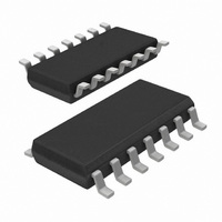
74ABT125D,623 NXP Semiconductors, 74ABT125D,623 Datasheet - Page 5

74ABT125D,623
Manufacturer Part Number
74ABT125D,623
Description
IC BUFF TRI-ST QD N-INV 14SOICN
Manufacturer
NXP Semiconductors
Series
74ABTr
Datasheet
1.74ABT125D623.pdf
(16 pages)
Specifications of 74ABT125D,623
Logic Type
Buffer/Line Driver, Non-Inverting
Number Of Elements
4
Number Of Bits Per Element
1
Current - Output High, Low
32mA, 64mA
Voltage - Supply
4.5 V ~ 5.5 V
Operating Temperature
-40°C ~ 85°C
Mounting Type
Surface Mount
Package / Case
14-SOIC (3.9mm Width), 14-SOL
Logic Family
ABT
Number Of Channels Per Chip
4
Polarity
Non-Inverting
Supply Voltage (max)
5.5 V
Supply Voltage (min)
4.5 V
Maximum Operating Temperature
+ 85 C
Mounting Style
SMD/SMT
High Level Output Current
- 32 mA
Low Level Output Current
64 mA
Minimum Operating Temperature
- 40 C
Number Of Lines (input / Output)
4 / 4
Output Type
3-State
Propagation Delay Time
4.6 ns at 5 V
Lead Free Status / RoHS Status
Lead free / RoHS Compliant
Other names
568-2279-2
74ABT125D-T
935056850623
74ABT125D-T
935056850623
NXP Semiconductors
Table 6.
[1]
[2]
[3]
10. Dynamic characteristics
Table 7.
GND = 0 V. Test circuit is shown in
74ABT125
Product data sheet
Symbol
I
C
C
Symbol Parameter
t
t
t
t
t
t
PLH
PHL
PZH
PZL
PHZ
PLZ
I
O
CC
This parameter is valid for any V
a transition time of up to 100 s is permitted.
Not more than one output should be tested at a time, and the duration of the test should not exceed one second.
This is the increase in supply current for each input at 3.4 V.
LOW to HIGH
propagation delay
HIGH to LOW
propagation delay
OFF-state to HIGH
propagation delay
OFF-state to LOW
propagation delay
HIGH to OFF-state
propagation delay
LOW to OFF-state
propagation delay
Parameter
additional supply
current
input capacitance
output capacitance
Static characteristics
Dynamic characteristics
Conditions
nA to nY, see
nA to nY; see
nOE to nY; see
nOE to nY; see
nOE to nY; see
nOE to nY; see
CC
…continued
Figure
Conditions
per control pin; V
one control input at 3.4 V, other
inputs at V
one enable input at 3.4 V and other
inputs at V
disabled
V
outputs disabled; V
between 0 V and 2.1 V, with a transition time of up to 10 ms. From V
I
outputs enabled
outputs disabled
= 0 V or V
8.
All information provided in this document is subject to legal disclaimers.
Figure 6
Figure 6
CC
CC
Figure 7
Figure 7
Figure 7
Figure 7
CC
Rev. 5 — 24 November 2010
or GND
or GND; outputs
CC
O
= 5.5 V;
= 0 V or V
CC
[3]
25 C; V
Min
1.0
1.0
1.0
1.0
1.0
1.5
25 C
Min
-
-
-
-
-
Typ
CC
2.8
3.1
3.2
4.2
4.1
2.8
Typ
0.5
0.5
50
= 5.0 V
4
7
Max
4.1
4.6
5.0
6.2
5.4
5.0
Max
250
1.5
1.5
-
-
CC
40 C to +85 C;
V
CC
40 C to +85 C Unit
= 2.1 V to V
Min
1.0
1.0
1.0
1.0
1.0
1.5
74ABT125
Quad buffer; 3-state
Min
= 5.0 V 0.5 V
-
-
-
-
-
© NXP B.V. 2010. All rights reserved.
CC
Max
Max
4.6
4.9
5.9
6.8
6.2
5.5
250
1.5
1.5
-
-
= 5 V 10 %,
mA
mA
mA
pF
pF
Unit
ns
ns
ns
ns
ns
ns
5 of 16


