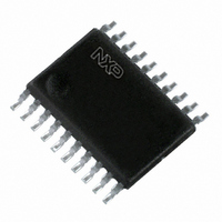
74AHCT541PW,112 NXP Semiconductors, 74AHCT541PW,112 Datasheet - Page 9

74AHCT541PW,112
Manufacturer Part Number
74AHCT541PW,112
Description
IC BUFF/DVR TRI-ST 8BIT 20TSSOP
Manufacturer
NXP Semiconductors
Series
74AHCTr
Datasheet
1.74AHC541PW118.pdf
(16 pages)
Specifications of 74AHCT541PW,112
Package / Case
20-TSSOP
Logic Type
Buffer/Line Driver, Non-Inverting
Number Of Elements
1
Number Of Bits Per Element
8
Current - Output High, Low
8mA, 8mA
Voltage - Supply
4.5 V ~ 5.5 V
Operating Temperature
-40°C ~ 125°C
Mounting Type
Surface Mount
Logic Family
AHCT
Number Of Channels Per Chip
8
Polarity
Non-Inverting
Supply Voltage (max)
5.5 V
Supply Voltage (min)
4.5 V
Maximum Operating Temperature
+ 125 C
Mounting Style
SMD/SMT
High Level Output Current
- 8 mA
Low Level Output Current
8 mA
Minimum Operating Temperature
- 40 C
Output Type
3-State
Propagation Delay Time
8.5 ns @ 5 V
Number Of Lines (input / Output)
8 / 8
Logical Function
Buffer/Line Driver
Number Of Elements
1
Number Of Channels
8
Number Of Inputs
8
Number Of Outputs
8
Operating Supply Voltage (typ)
5V
Package Type
TSSOP
Operating Supply Voltage (max)
5.5V
Operating Supply Voltage (min)
4.5V
Quiescent Current
4uA
Technology
CMOS
Pin Count
20
Mounting
Surface Mount
Operating Temp Range
-40C to 125C
Operating Temperature Classification
Automotive
Lead Free Status / RoHS Status
Lead free / RoHS Compliant
Lead Free Status / RoHS Status
Lead free / RoHS Compliant, Lead free / RoHS Compliant
Other names
568-4467-5
74AHCT541PW
74AHCT541PW
935261978112
74AHCT541PW
74AHCT541PW
935261978112
NXP Semiconductors
11. Waveforms
Table 8.
74AHC_AHCT541_3
Product data sheet
Type
74AHC541
74AHCT541
Fig 5. Propagation delay input (An) to output (Yn)
Fig 6. Enable and disable times
Measurement points are given in
V
Measurement points are given in
V
OL
OL
Measurement points
and V
and V
OH
OH
are typical voltage output levels that occur with the output load.
are typical voltage output levels that occur with the output load.
HIGH-to-OFF
OFF-to-HIGH
LOW-to-OFF
OFF-to-LOW
OEn input
output
output
Yn output
Input
V
0.5V
1.5 V
An input
M
Table
Table
GND
GND
V
V
V
OH
CC
OL
V
CC
I
8.
8.
GND
V
V
OH
OL
Rev. 03 — 12 November 2007
V
I
V
enabled
outputs
M
t
PLZ
t
PHZ
V
V
Output
V
0.5V
0.5V
M
X
M
V
V
Y
M
t
CC
CC
PHL
74AHC541; 74AHCT541
disabled
outputs
t
PZL
t
PZH
mna901
V
V
V
t
X
OL
OL
PLH
V
M
+ 0.3 V
+ 0.3 V
V
Octal buffer/line driver; 3-state
M
enabled
outputs
mna902
V
V
V
© NXP B.V. 2007. All rights reserved.
Y
OH
OH
0.3 V
0.3 V
9 of 16


