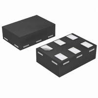
74AUP2G07GM,132 NXP Semiconductors, 74AUP2G07GM,132 Datasheet - Page 5

74AUP2G07GM,132
Manufacturer Part Number
74AUP2G07GM,132
Description
IC BUFF DL LOW PWR OP/DR 6XSON
Manufacturer
NXP Semiconductors
Series
74AUPr
Datasheet
1.74AUP2G07GW125.pdf
(18 pages)
Specifications of 74AUP2G07GM,132
Logic Type
Buffer/Line Driver, Non-Inverting with Open Drain
Number Of Elements
2
Number Of Bits Per Element
1
Current - Output High, Low
4mA, 4mA
Voltage - Supply
0.8 V ~ 3.6 V
Operating Temperature
-40°C ~ 125°C
Mounting Type
Surface Mount
Package / Case
6-XSON (Micropak™), SOT-886
Lead Free Status / RoHS Status
Lead free / RoHS Compliant
Other names
74AUP2G07GM-H
74AUP2G07GM-H
935279986132
74AUP2G07GM-H
935279986132
NXP Semiconductors
Table 7.
At recommended operating conditions; voltages are referenced to GND (ground = 0 V).
74AUP2G07
Product data sheet
Symbol Parameter
V
I
I
I
ΔI
I
ΔI
C
C
T
V
V
V
I
I
I
OZ
OFF
CC
I
OZ
amb
OL
IH
IL
OL
I
O
OFF
CC
= −40 °C to +85 °C
LOW-level output voltage
input leakage current
OFF-state output current
power-off leakage current
additional power-off
leakage current
supply current
additional supply current
input capacitance
output capacitance
HIGH-level input voltage
LOW-level input voltage
LOW-level output voltage
input leakage current
OFF-state output current
Static characteristics
…continued
Conditions
V
V
V
to 3.6 V
V
V
V
V
V
V
V
V
V
V
V
V
V
V
V
V
V
V
V
to 3.6 V
I
I
I
I
I
CC
I
CC
I
CC
O
CC
CC
CC
CC
CC
CC
CC
CC
I
I
I
I
I
I
I
I
I
I
I
I
I
I
I
I
I
I
I
= V
= V
= GND to 3.6 V; V
= V
or V
or V
= GND or V
= V
= GND to 3.6 V; V
= V
O
O
O
O
O
O
O
O
O
O
O
O
O
O
O
O
= GND; V
All information provided in this document is subject to legal disclaimers.
= 0 V to 0.2 V
= 0.8 V to 3.6 V
= 0 V to 3.6 V; V
= 0.8 V
= 0.9 V to 1.95 V
= 2.3 V to 2.7 V
= 3.0 V to 3.6 V
= 0.8 V
= 0.9 V to 1.95 V
= 2.3 V to 2.7 V
= 3.0 V to 3.6 V
= 20 μA; V
= 1.1 mA; V
= 1.7 mA; V
= 1.9 mA; V
= 2.3 mA; V
= 3.1 mA; V
= 2.7 mA; V
= 4.0 mA; V
= 20 μA; V
= 1.1 mA; V
= 1.7 mA; V
= 1.9 mA; V
= 2.3 mA; V
= 3.1 mA; V
= 2.7 mA; V
= 4.0 mA; V
CC
IH
IH
IH
IH
O
O
; V
; V
or V
or V
= 0 V to 3.6 V; V
= 0 V to 3.6 V;
− 0.6 V; I
Rev. 5 — 9 September 2010
O
O
= 0 V to 3.6 V; V
= 0 V to 3.6 V; V
IL
IL
CC
CC
CC
CC
= 0 V
CC
CC
CC
CC
CC
CC
CC
CC
CC
CC
CC
CC
CC
CC
; I
O
= 0.8 V to 3.6 V
O
= 0.8 V to 3.6 V
= 0 A; V
= 1.1 V
= 1.4 V
= 1.65 V
= 2.3 V
= 2.3 V
= 3.0 V
= 3.0 V
= 1.1 V
= 1.4 V
= 1.65 V
= 2.3 V
= 2.3 V
= 3.0 V
= 3.0 V
CC
= 0 A;
CC
I
= GND or V
= 0 V to 3.6 V
= 0 V to 3.6 V
CC
CC
= 0 V
CC
CC
Low-power dual buffer with open-drain output
= 3.3 V
= 0 V
= 0 V
CC
Min
-
-
-
-
-
-
-
-
-
-
-
-
-
-
-
-
-
-
-
-
-
-
-
-
0.70 × V
0.65 × V
1.6
2.0
-
-
-
-
-
-
CC
CC
74AUP2G07
Typ
-
-
-
-
-
-
-
-
-
-
-
-
-
-
0.7
0.9
-
-
-
-
-
-
-
-
-
-
-
-
-
-
-
-
-
-
© NXP B.V. 2010. All rights reserved.
Max
0.3 × V
0.31
0.31
0.31
0.44
0.31
0.44
±0.1
±0.1
±0.2
±0.2
0.5
40
-
-
-
-
0.3 × V
0.37
0.35
0.33
0.45
0.33
0.45
±0.5
±0.5
0.1
-
-
0.30 × V
0.35 × V
0.7
0.9
0.1
CC
CC
CC
CC
5 of 18
Unit
V
V
V
V
V
V
V
V
μA
μA
μA
μA
μA
μA
pF
pF
V
V
V
V
V
V
V
V
V
V
V
V
V
V
V
V
μA
μA


