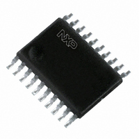
74LVC244APW,112 NXP Semiconductors, 74LVC244APW,112 Datasheet - Page 7

74LVC244APW,112
Manufacturer Part Number
74LVC244APW,112
Description
IC BUFF/DVR TRI-ST DUAL 20TSSOP
Manufacturer
NXP Semiconductors
Series
74LVCr
Datasheet
1.74LVC244APW118.pdf
(18 pages)
Specifications of 74LVC244APW,112
Package / Case
20-TSSOP
Logic Type
Buffer/Line Driver, Non-Inverting
Number Of Elements
2
Number Of Bits Per Element
4
Current - Output High, Low
24mA, 24mA
Voltage - Supply
1.2 V ~ 3.6 V
Operating Temperature
-40°C ~ 125°C
Mounting Type
Surface Mount
Logic Family
LVC
Number Of Channels Per Chip
8
Polarity
Non-Inverting
Supply Voltage (max)
3.6 V
Supply Voltage (min)
1.2 V
Maximum Operating Temperature
+ 125 C
Mounting Style
SMD/SMT
High Level Output Current
- 24 mA
Input Bias Current (max)
40 uA
Low Level Output Current
24 mA
Maximum Power Dissipation
500 mW
Minimum Operating Temperature
- 40 C
Output Current
50 mA
Output Type
3-State
Output Voltage
6.5 V
Propagation Delay Time
2.8 ns (Typ) @ 3.3 V
Number Of Lines (input / Output)
8 / 8
Logical Function
Buffer/Line Driver
Number Of Elements
2
Number Of Channels
8
Number Of Inputs
8
Number Of Outputs
8
Operating Supply Voltage (typ)
1.8/2.5/3.3V
Package Type
TSSOP
Operating Supply Voltage (max)
3.6V
Operating Supply Voltage (min)
1.2V
Quiescent Current
40uA
Technology
CMOS
Pin Count
20
Mounting
Surface Mount
Operating Temp Range
-40C to 125C
Operating Temperature Classification
Automotive
Lead Free Status / RoHS Status
Lead free / RoHS Compliant
Lead Free Status / RoHS Status
Lead free / RoHS Compliant, Lead free / RoHS Compliant
Other names
568-5001
74LVC244APW
74LVC244APW,112
74LVC244APW
935210420112
74LVC244APW
74LVC244APW,112
74LVC244APW
935210420112
NXP Semiconductors
Table 6.
At recommended operating conditions. Voltages are referenced to GND (ground = 0 V).
[1]
[2]
[3]
[4]
[5]
[6]
10. Dynamic characteristics
Table 7.
Voltages are referenced to GND (ground = 0 V). For test circuit see
74LVC_LVCH244A_6
Product data sheet
Symbol Parameter
C
I
I
I
I
Symbol Parameter
t
t
t
t
BHL
BHH
BHLO
BHHO
pd
en
dis
sk(o)
I
All typical values are measured at V
The bus hold circuit is switched off when V
For I/O ports the parameter I
Valid for data inputs of bus hold parts only (74LVCH244A). Note that control inputs do not have a bus hold circuit.
The specified sustaining current at the data input holds the input below the specified V
The specified overdrive current at the data input forces the data input to the opposite input state.
propagation
delay
enable time
disable time
output skew
time
input capacitance
bus hold LOW
current
bus hold HIGH
current
bus hold LOW
overdrive current
bus hold HIGH
overdrive current
Static characteristics
Dynamic characteristics
Conditions
nAn to nYn; see
nOE to nYn; see
nOE to nYn; see
V
V
V
V
V
V
V
V
V
OZ
CC
CC
CC
CC
CC
CC
CC
CC
CC
Conditions
V
V
V
V
CC
CC
CC
CC
includes the input leakage current.
= 1.2 V
= 2.7 V
= 3.0 V to 3.6 V
= 1.2 V
= 2.7 V
= 3.0 V to 3.6 V
= 1.2 V
= 2.7 V
= 3.0 V to 3.6 V
= 3.0 V; V
= 3.0 V; V
= 3.6 V
= 3.6 V
…continued
CC
= 3.3 V (unless stated otherwise) and T
I
Figure 6
> V
Figure 7
Figure 7
I
I
= 0.8 V
= 2.0 V
CC
allowing 5.5 V on the input terminal.
Rev. 06 — 13 August 2009
74LVC244A; 74LVCH244A
[4][5]
[4][5]
[4][6]
[4][6]
Figure
[1]
[3]
[1]
[3]
[1]
[3]
[4]
Min
500
75
500
75
Min
-
1.5
1.5
1.5
1.0
1.5
1.5
amb
8.
40 C to +85 C
-
-
-
-
40 C to +85 C
= 25 C.
I
Typ
Typ
17.0
24.0
level.
3.3
2.8
3.3
3.4
9.0
3.2
2.9
4.0
-
-
-
-
-
[2]
[1]
Octal buffer/line driver; 3-state
Max
Max
6.9
5.9
8.6
7.6
6.8
5.8
1.0
-
-
-
-
-
-
-
-
40 C to +125 C Unit
40 C to +125 C Unit
Min
1.5
1.5
1.5
1.0
1.5
1.5
Min
500
60
500
-
-
-
-
60
-
© NXP B.V. 2009. All rights reserved.
Max
Max
9.0
7.5
9.5
8.5
7.5
1.5
11
-
-
-
-
-
-
-
-
pF
7 of 18
ns
ns
ns
ns
ns
ns
ns
ns
ns
ns
A
A
A
A


