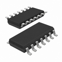
N74F125D,623 NXP Semiconductors, N74F125D,623 Datasheet - Page 4

N74F125D,623
Manufacturer Part Number
N74F125D,623
Description
IC BUFFER TRI-ST QUAD 14SOICN
Manufacturer
NXP Semiconductors
Series
74Fr
Datasheet
1.N74F126D623.pdf
(10 pages)
Specifications of N74F125D,623
Logic Type
Buffer/Line Driver, Non-Inverting
Number Of Elements
4
Number Of Bits Per Element
1
Current - Output High, Low
15mA, 64mA
Voltage - Supply
4.5 V ~ 5.5 V
Operating Temperature
0°C ~ 70°C
Mounting Type
Surface Mount
Package / Case
14-SOIC (3.9mm Width), 14-SOL
Logic Family
F
Number Of Channels Per Chip
4
Polarity
Non-Inverting
Supply Voltage (max)
5.5 V
Supply Voltage (min)
4.5 V
Maximum Operating Temperature
+ 70 C
Mounting Style
SMD/SMT
High Level Output Current
- 15 mA
Low Level Output Current
64 mA
Minimum Operating Temperature
0 C
Number Of Lines (input / Output)
4 / 4
Output Type
3-State
Propagation Delay Time
7.5 ns at 5 V
Lead Free Status / RoHS Status
Lead free / RoHS Compliant
Other names
568-2322-2
933784210623
N74F125D-T
933784210623
N74F125D-T
1. For conditions shown as MIN or MAX, use the appropriate value specified under recommended operating conditions for the applicable type.
2. All typical values are at V
3. Not more than one output should be shorted at a time. For testing I
Philips Semiconductors
RECOMMENDED OPERATING CONDITIONS
DC ELECTRICAL CHARACTERISTICS
(Over recommended operating free-air temperature range unless otherwise noted.)
NOTES:
March 28, 1989
V
V
V
I
I
I
T
V
V
V
V
V
I
I
I
I
I
I
I
I
IK
OH
OL
I
IH
IL
OZH
OZL
OS
CC
CC
SYMBOL
SYMBOL
SYMBOL
SYMBOL
amb
CC
IH
IL
O
OH
O
OL
IK
Quad buffers (3-State)
techniques are preferable in order to minimize internal heating and more accurately reflect operational values. Otherwise, prolonged shorting
of a High output may raise the chip temperature well above normal and thereby cause invalid readings in other parameter tests. In any
sequence of parameter tests, I
Supply voltage
High-level input voltage
Low-level input voltage
Input clamp current
High-level output current
Low-level output current
Operating free air temperature range
High level output voltage
High-level output voltage
Low level output voltage
Low-level output voltage
Input clamp voltage
Input current at maximum input voltage
High-level input current
Low-level input current
Off-state output current,
High-level voltage applied
Off-state output current,
Low-level voltage applied
Short circuit output current
Supply current (total)
Supply current (total)
PARAMETER
PARAMETER
CC
= 5V, T
OS
tests should be performed last.
amb
74F125
74F126
3
= 25 C.
PARAMETER
PARAMETER
I
I
I
I
I
I
CCH
CCL
CCZ
CCH
CCL
CCZ
V
V
V
V
V
V
V
V
V
V
V
V
V
V
V
V
V
CC
IL
IL
IH
CC
IL
IL
IH
CC
CC
CC
CC
CC
CC
CC
CC
CC
= MAX
= MAX,
= MAX
= MAX,
= MIN
= MIN
= MIN,
= MIN,
= MIN, I
= 0.0V, V
= MAX, V
= MAX, V
= MAX, V
= MAX, V
= MAX
= MAX
= MAX
TEST CONDITIONS
TEST CONDITIONS
OS
4
I
, the use of high-speed test apparatus and/or sample-and-hold
= I
I
I
I
O
O
= 7.0V
= 2.7V
= 0.5V
= 2.7V
= 0.5V
IK
I
I
I
I
I
I
OEn = GND, Dn = 4.5V
OEn = Dn = GND
OEn = Dn = 4.5V
OEn = Dn = 4.5V
OEn = 4.5V, Dn = GND
OEn = GND, Dn = 4.5V
O
OH
O
OH
O
OH
= 3mA
=–3mA
= 15mA
=–15mA
= MAX
= MAX
1
1
10%V
5%V
10%V
5%V
10%V
5%V
MIN
4.5
2.0
0
CC
CC
CC
CC
CC
CC
–100
LIMITS
MIN
2.4
2.7
2.0
2.0
NOM
5.0
74F125, 74F126
LIMITS
–0.73
TYP
0.42
3.3
17
28
25
20
32
26
2
MAX
–18
–15
+70
5.5
0.8
64
Product specification
MAX
–225
0.55
0.55
–1.2
100
–20
–50
20
50
24
40
35
30
48
39
UNIT
UNIT
mA
mA
mA
V
V
V
UNIT
UNIT
C
mA
mA
mA
mA
mA
mA
mA
V
V
V
V
V
V
V
A
A
A
A
A


