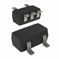
74HC1G126GW,125 NXP Semiconductors, 74HC1G126GW,125 Datasheet - Page 4

74HC1G126GW,125
Manufacturer Part Number
74HC1G126GW,125
Description
IC BUS BUFF DVR TRI-ST 5TSSOP
Manufacturer
NXP Semiconductors
Series
74HCr
Datasheet
1.74HCT1G126GV125.pdf
(12 pages)
Specifications of 74HC1G126GW,125
Package / Case
SC-70-5, SC-88A, SOT-323-5, SOT-353, 5-TSSOP
Logic Type
Buffer/Line Driver, Non-Inverting
Number Of Elements
1
Number Of Bits Per Element
1
Current - Output High, Low
7.8mA, 7.8mA
Voltage - Supply
2 V ~ 6 V
Operating Temperature
-40°C ~ 125°C
Mounting Type
Surface Mount
Logic Family
HC
Number Of Channels Per Chip
1
Polarity
Non-Inverting
Supply Voltage (max)
6 V
Supply Voltage (min)
2 V
Maximum Operating Temperature
+ 125 C
Mounting Style
SMD/SMT
High Level Output Current
- 7.8 mA
Low Level Output Current
7.8 mA
Minimum Operating Temperature
- 40 C
Output Type
3-State
Propagation Delay Time
24 ns (Typ) @ 2 V or 10 ns (Typ) @ 4.5 V or 9 ns (Typ) @ 6 V
Number Of Lines (input / Output)
1 / 1
Logical Function
Buffer/Line Driver
Number Of Elements
1
Number Of Channels
1
Number Of Inputs
1
Number Of Outputs
1
Operating Supply Voltage (typ)
5V
Package Type
TSSOP
Operating Supply Voltage (max)
6V
Operating Supply Voltage (min)
2V
Quiescent Current
20uA
Technology
CMOS
Pin Count
5
Mounting
Surface Mount
Operating Temp Range
-40C to 125C
Operating Temperature Classification
Automotive
Lead Free Status / RoHS Status
Lead free / RoHS Compliant
Lead Free Status / RoHS Status
Lead free / RoHS Compliant, Lead free / RoHS Compliant
Other names
74HC1G126GW-G
74HC1G126GW-G
935245710125
74HC1G126GW-G
935245710125
NXP Semiconductors
Table 7.
Voltages are referenced to GND (ground = 0 V). All typical values are measured at T
74HC_HCT1G126_4
Product data sheet
Symbol
V
V
I
I
I
C
For type 74HCT1G126
V
V
V
V
I
I
I
C
I
OZ
CC
I
OZ
CC
I
OH
OL
IH
IL
OH
OL
I
I
CC
Static characteristics
Parameter
HIGH-level output
voltage
LOW-level output
voltage
input leakage current
OFF-state output
current
supply current
input capacitance
HIGH-level input
voltage
LOW-level input
voltage
HIGH-level output
voltage
LOW-level output
voltage
input leakage current
OFF-state output
current
supply current
additional supply
current
input capacitance
…continued
Conditions
V
V
V
V
GND; V
V
V
V
V
V
V
V
V
GND; V
V
V
per input; V
V
I
I
I
I
I
CC
CC
CC
I
I
I
I
I
CC
I
I
I
I
I
I
I
I
I
I
I
I
I
I
I
= V
= V
= V
= V
= V
= V
= V
= V
= V
= V
= V
O
O
O
O
O
O
O
O
O
O
O
O
O
O
= 4.5 V to 5.5 V
= 4.5 V to 5.5 V
= 6.0 V
= 5.5 V
= 20 A; V
= 20 A; V
= 20 A; V
= 6.0 mA; V
= 7.8 mA; V
= 20 A; V
= 20 A; V
= 20 A; V
= 6.0 mA; V
= 7.8 mA; V
= 20 A
= 6.0 mA
= 20 A
= 6.0 mA
IH
IH
CC
IH
CC
IH
IH
CC
IH
CC
CC
CC
CC
or V
or V
or V
or V
or V
or V
or GND; V
or GND; I
or GND; V
or GND; I
= 6.0 V
= 5.5 V
2.1 V; I
CC
IL
IL
IL
IL
IL
IL
; V
; V
; V
; V
= 4.5 V to 5.5 V;
Rev. 04 — 20 July 2007
CC
CC
CC
CC
CC
CC
CC
CC
O
CC
CC
O
CC
CC
O
= 2.0 V
= 4.5 V
= 6.0 V
= V
O
= V
O
CC
= 4.5 V
= 4.5 V
CC
= 2.0 V
= 4.5 V
= 6.0 V
= 4.5 V
= 6.0 V
= 0 A
= 0 A;
= 0 A;
= 4.5 V
= 6.0 V
CC
CC
= 6.0 V
= 5.5 V
or
or
74HC1G126; 74HCT1G126
3.84
5.34
3.84
Min
1.9
4.4
5.9
2.0
4.4
-
-
-
-
-
-
-
-
-
-
-
-
-
-
-
-
-
40 C to +85 C
4.32
5.81
0.15
0.16
4.32
0.16
Typ
2.0
4.5
6.0
1.5
1.6
1.2
4.5
1.5
0
0
0
0
-
-
-
-
-
-
-
amb
Max
0.33
0.33
0.33
500
0.1
0.1
0.1
1.0
0.8
0.1
1.0
= 25 C.
10
10
5
5
-
-
-
-
-
-
-
-
-
-
Bus buffer/line driver; 3-state
Min
40 C to +125 C
1.9
4.4
5.9
3.7
5.2
2.0
4.4
3.7
-
-
-
-
-
-
-
-
-
-
-
-
-
-
-
-
-
© NXP B.V. 2007. All rights reserved.
Max
850
0.1
0.1
0.1
0.4
0.4
1.0
0.8
0.1
0.4
1.0
10
20
10
20
-
-
-
-
-
-
-
-
-
-
Unit
V
V
V
V
V
V
V
V
V
V
pF
V
V
V
V
V
V
pF
4 of 12
A
A
A
A
A
A


