74LVC07APW,118 NXP Semiconductors, 74LVC07APW,118 Datasheet - Page 2
74LVC07APW,118
Manufacturer Part Number
74LVC07APW,118
Description
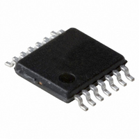
IC BUFF HEX OPEN DRAIN 14TSSOP
Manufacturer
NXP Semiconductors
Series
74LVCr
Datasheet
1.74LVC07ABQ115.pdf
(14 pages)
Specifications of 74LVC07APW,118
Logic Type
Buffer/Line Driver, Non-Inverting with Open Drain
Package / Case
14-TSSOP
Number Of Elements
6
Number Of Bits Per Element
1
Current - Output High, Low
32mA, 32mA
Voltage - Supply
2 V ~ 5.5 V
Operating Temperature
-40°C ~ 125°C
Mounting Type
Surface Mount
Logic Family
74LVC
Number Of Channels Per Chip
6
Polarity
Non-Inverting
Supply Voltage (max)
5.5 V
Supply Voltage (min)
1.65 V
Maximum Operating Temperature
125 C
Mounting Style
SMD/SMT
Input Bias Current (max)
10 uA
Low Level Output Current
32 mA
Maximum Power Dissipation
500 mW
Minimum Operating Temperature
- 40 C
Number Of Lines (input / Output)
6 / 6
Output Type
Open Drain
Propagation Delay Time
2.5 ns
Logical Function
Buffer/Driver
Number Of Elements
6
Number Of Channels
6
Number Of Inputs
6
Number Of Outputs
6
Operating Supply Voltage (typ)
1.8/2.5/3.3/5V
Package Type
TSSOP
High Level Output Current
32mA
Operating Supply Voltage (max)
5.5V
Operating Supply Voltage (min)
1.65V
Quiescent Current
10uA
Technology
CMOS
Pin Count
14
Mounting
Surface Mount
Operating Temp Range
-40C to 125C
Operating Temperature Classification
Automotive
Lead Free Status / RoHS Status
Lead free / RoHS Compliant
Lead Free Status / RoHS Status
Lead free / RoHS Compliant, Lead free / RoHS Compliant
Other names
568-2286-2
74LVC07APW-T
935265482118
74LVC07APW-T
935265482118


Philips Semiconductors
FEATURES
QUICK REFERENCE DATA
GND = 0 V; T
Note
1. C
2. The condition is V
FUNCTION TABLE
See note 1.
Note
1. H = HIGH voltage level;
2003 Nov 11
t
C
C
PLZ
5 V tolerant inputs and outputs (open drain) for
interfacing with 5 V logic
Wide supply voltage range from 1.65 to 5.5 V
CMOS low power consumption
Direct interface with TTL levels
Inputs accept voltages up to 5 V
Complies with JEDEC standard no. 8-1A
ESD protection:
HBM EIA/JESD22-A114-A exceeds 2000 V
MM EIA/JESD22-A115-A exceeds 200 V.
I
PD
Hex buffer with open-drain outputs
SYMBOL
P
f
f
C
V
N = total load switching outputs;
L = LOW voltage level;
Z = high-impedance OFF-state.
/t
i
o
(C
D
CC
PD
= input frequency in MHz;
L
PZL
= output frequency in MHz;
= output load capacitance in pF;
= C
L
is used to determine the dynamic power dissipation (P
= supply voltage in Volts;
PD
V
CC
amb
2
V
CC
= 25 C; t
propagation delay nA to nY
input capacitance
power dissipation capacitance per gate
f
o
2
) = sum of the outputs.
I
f
= GND to V
i
INPUT
N + (C
r
= t
nA
H
L
f
PARAMETER
2.5 ns.
L
CC
V
CC
2
f
o
) where:
2
C
V
DESCRIPTION
The 74LVC07A is a high-performance, low-power,
low-voltage, Si-gate CMOS device, superior to most
advanced CMOS compatible TTL families. Inputs can be
driven from either 3.3 or 5 V devices. This feature allows
the use of these devices as translators in a mixed
3.3 to 5 V environment.
The 74LVC07A provides six non-inverting buffers.
The outputs of the 74LVC07A are open drain and can be
connected to other open-drain outputs to implement
active-LOW wired-OR or active-HIGH wired-AND
functions.
CC
L
D
= 50 pF; V
in W).
= 3.3 V; notes 1 and 2
CONDITIONS
CC
= 3.3 V
OUTPUT
nY
L
Z
2.2
5.0
6.0
TYPICAL
Product specification
74LVC07A
ns
pF
pF
UNIT
Related parts for 74LVC07APW,118
Image
Part Number
Description
Manufacturer
Datasheet
Request
R

Part Number:
Description:
NXP Semiconductors designed the LPC2420/2460 microcontroller around a 16-bit/32-bitARM7TDMI-S CPU core with real-time debug interfaces that include both JTAG andembedded trace
Manufacturer:
NXP Semiconductors
Datasheet:

Part Number:
Description:
NXP Semiconductors designed the LPC2458 microcontroller around a 16-bit/32-bitARM7TDMI-S CPU core with real-time debug interfaces that include both JTAG andembedded trace
Manufacturer:
NXP Semiconductors
Datasheet:
Part Number:
Description:
NXP Semiconductors designed the LPC2468 microcontroller around a 16-bit/32-bitARM7TDMI-S CPU core with real-time debug interfaces that include both JTAG andembedded trace
Manufacturer:
NXP Semiconductors
Datasheet:
Part Number:
Description:
NXP Semiconductors designed the LPC2470 microcontroller, powered by theARM7TDMI-S core, to be a highly integrated microcontroller for a wide range ofapplications that require advanced communications and high quality graphic displays
Manufacturer:
NXP Semiconductors
Datasheet:
Part Number:
Description:
NXP Semiconductors designed the LPC2478 microcontroller, powered by theARM7TDMI-S core, to be a highly integrated microcontroller for a wide range ofapplications that require advanced communications and high quality graphic displays
Manufacturer:
NXP Semiconductors
Datasheet:
Part Number:
Description:
The Philips Semiconductors XA (eXtended Architecture) family of 16-bit single-chip microcontrollers is powerful enough to easily handle the requirements of high performance embedded applications, yet inexpensive enough to compete in the market for hi
Manufacturer:
NXP Semiconductors
Datasheet:
Part Number:
Description:
The XA-S3 device is a member of Philips Semiconductors? XA(eXtended Architecture) family of high performance 16-bitsingle-chip microcontrollers
Manufacturer:
NXP Semiconductors
Datasheet:

Part Number:
Description:
The NXP BlueStreak LH75401/LH75411 family consists of two low-cost 16/32-bit System-on-Chip (SoC) devices
Manufacturer:
NXP Semiconductors
Datasheet:
Part Number:
Description:
The NXP LPC3130/3131 combine an 180 MHz ARM926EJ-S CPU core, high-speed USB2
Manufacturer:
NXP Semiconductors
Datasheet:
Part Number:
Description:
The NXP LPC3141 combine a 270 MHz ARM926EJ-S CPU core, High-speed USB 2
Manufacturer:
NXP Semiconductors
Part Number:
Description:
The NXP LPC3143 combine a 270 MHz ARM926EJ-S CPU core, High-speed USB 2
Manufacturer:
NXP Semiconductors

Part Number:
Description:
The NXP LPC3152 combines an 180 MHz ARM926EJ-S CPU core, High-speed USB 2
Manufacturer:
NXP Semiconductors
Part Number:
Description:
The NXP LPC3154 combines an 180 MHz ARM926EJ-S CPU core, High-speed USB 2
Manufacturer:
NXP Semiconductors

Part Number:
Description:
Standard level N-channel enhancement mode Field-Effect Transistor (FET) in a plastic package using NXP High-Performance Automotive (HPA) TrenchMOS technology
Manufacturer:
NXP Semiconductors
Datasheet: