74LVC125ADB,118 NXP Semiconductors, 74LVC125ADB,118 Datasheet - Page 4
74LVC125ADB,118
Manufacturer Part Number
74LVC125ADB,118
Description
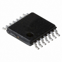
IC BUFF DVR TRI-ST QD 14SSOP
Manufacturer
NXP Semiconductors
Series
74LVCr
Datasheet
1.74LVC125ABQ115.pdf
(20 pages)
Specifications of 74LVC125ADB,118
Logic Type
Buffer/Line Driver, Non-Inverting
Package / Case
14-SSOP
Number Of Elements
4
Number Of Bits Per Element
1
Current - Output High, Low
24mA, 24mA
Voltage - Supply
2.7 V ~ 3.6 V
Operating Temperature
-40°C ~ 125°C
Mounting Type
Surface Mount
Logic Family
74LVC
Number Of Channels Per Chip
4
Polarity
Non-Inverting
Supply Voltage (max)
3.6 V
Supply Voltage (min)
1.2 V
Maximum Operating Temperature
125 C
Mounting Style
SMD/SMT
High Level Output Current
- 24 mA
Input Bias Current (max)
40 uA
Low Level Output Current
24 mA
Maximum Power Dissipation
500 mW
Minimum Operating Temperature
- 40 C
Number Of Lines (input / Output)
8 / 4
Output Type
3-State
Propagation Delay Time
2.4 ns
Lead Free Status / RoHS Status
Lead free / RoHS Compliant
Lead Free Status / RoHS Status
Lead free / RoHS Compliant, Lead free / RoHS Compliant
Other names
568-2277-2
74LVC125ADB-T
935231710118
74LVC125ADB-T
935231710118


Philips Semiconductors
2003 May 07
handbook, halfpage
handbook, halfpage
Quad buffer/line driver with 5 V tolerant input/outputs;
3-state
(1) The die substrate is attached to this pad using conductive die
attach material. It can not be used as a supply pin or input.
2OE
Fig.2 Pin configuration DHVQFN14.
1A
1Y
2A
2Y
Fig.4 Logic symbol (IEEE/IEC).
Top view
2
3
4
5
6
10
12
13
1
4
2
5
9
GND
1OE
EN1
7
1
GND
MNA229
V CC
1
(1)
3Y
14
8
11
MCE181
3
6
8
13
12
11
10
9
4OE
4A
4Y
3OE
3A
4
handbook, halfpage
handbook, halfpage
nOE
nA
Fig.5 Logic diagram.
Fig.3 Logic symbol.
10
12
13
2
1
5
4
9
1OE
2OE
3OE
4OE
1A
2A
3A
4A
MNA228
1Y
2Y
3Y
4Y
11
Product specification
3
6
8
74LVC125A
MNA227
nY
Related parts for 74LVC125ADB,118
Image
Part Number
Description
Manufacturer
Datasheet
Request
R

Part Number:
Description:
Quad buffer/line driver with 5-volt tolerant inputs/outputs 3-State
Manufacturer:
PHILIPS [NXP Semiconductors]
Datasheet:

Part Number:
Description:
Manufacturer:
NXP Semiconductors
Datasheet:
Part Number:
Description:
NXP Semiconductors designed the LPC2420/2460 microcontroller around a 16-bit/32-bitARM7TDMI-S CPU core with real-time debug interfaces that include both JTAG andembedded trace
Manufacturer:
NXP Semiconductors
Datasheet:

Part Number:
Description:
NXP Semiconductors designed the LPC2458 microcontroller around a 16-bit/32-bitARM7TDMI-S CPU core with real-time debug interfaces that include both JTAG andembedded trace
Manufacturer:
NXP Semiconductors
Datasheet:
Part Number:
Description:
NXP Semiconductors designed the LPC2468 microcontroller around a 16-bit/32-bitARM7TDMI-S CPU core with real-time debug interfaces that include both JTAG andembedded trace
Manufacturer:
NXP Semiconductors
Datasheet:
Part Number:
Description:
NXP Semiconductors designed the LPC2470 microcontroller, powered by theARM7TDMI-S core, to be a highly integrated microcontroller for a wide range ofapplications that require advanced communications and high quality graphic displays
Manufacturer:
NXP Semiconductors
Datasheet:
Part Number:
Description:
NXP Semiconductors designed the LPC2478 microcontroller, powered by theARM7TDMI-S core, to be a highly integrated microcontroller for a wide range ofapplications that require advanced communications and high quality graphic displays
Manufacturer:
NXP Semiconductors
Datasheet:
Part Number:
Description:
The Philips Semiconductors XA (eXtended Architecture) family of 16-bit single-chip microcontrollers is powerful enough to easily handle the requirements of high performance embedded applications, yet inexpensive enough to compete in the market for hi
Manufacturer:
NXP Semiconductors
Datasheet:
Part Number:
Description:
The XA-S3 device is a member of Philips Semiconductors? XA(eXtended Architecture) family of high performance 16-bitsingle-chip microcontrollers
Manufacturer:
NXP Semiconductors
Datasheet:

Part Number:
Description:
The NXP BlueStreak LH75401/LH75411 family consists of two low-cost 16/32-bit System-on-Chip (SoC) devices
Manufacturer:
NXP Semiconductors
Datasheet:
Part Number:
Description:
The NXP LPC3130/3131 combine an 180 MHz ARM926EJ-S CPU core, high-speed USB2
Manufacturer:
NXP Semiconductors
Datasheet:
Part Number:
Description:
The NXP LPC3141 combine a 270 MHz ARM926EJ-S CPU core, High-speed USB 2
Manufacturer:
NXP Semiconductors
Part Number:
Description:
The NXP LPC3143 combine a 270 MHz ARM926EJ-S CPU core, High-speed USB 2
Manufacturer:
NXP Semiconductors

Part Number:
Description:
The NXP LPC3152 combines an 180 MHz ARM926EJ-S CPU core, High-speed USB 2
Manufacturer:
NXP Semiconductors