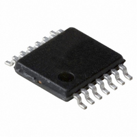
74AHC125PW,118 NXP Semiconductors, 74AHC125PW,118 Datasheet - Page 3

74AHC125PW,118
Manufacturer Part Number
74AHC125PW,118
Description
IC BUFF DVR TRI-ST QD 14TSSOP
Manufacturer
NXP Semiconductors
Series
74AHCr
Datasheet
1.74AHC125PW118.pdf
(15 pages)
Specifications of 74AHC125PW,118
Package / Case
14-TSSOP
Logic Type
Buffer/Line Driver, Non-Inverting
Number Of Elements
4
Number Of Bits Per Element
1
Current - Output High, Low
8mA, 8mA
Voltage - Supply
2 V ~ 5.5 V
Operating Temperature
-40°C ~ 125°C
Mounting Type
Surface Mount
Logic Family
AHC
Number Of Channels Per Chip
4
Polarity
Non-Inverting
Supply Voltage (max)
5.5 V
Supply Voltage (min)
2 V
Maximum Operating Temperature
+ 125 C
Mounting Style
SMD/SMT
High Level Output Current
- 8 mA
Low Level Output Current
8 mA
Minimum Operating Temperature
- 40 C
Output Type
3-State
Propagation Delay Time
11.5 ns @ 3 V to 3.6 V or 7.5 ns @ 4.5 V to 5.5 V
Number Of Lines (input / Output)
4 / 4
Lead Free Status / RoHS Status
Lead free / RoHS Compliant
Lead Free Status / RoHS Status
Lead free / RoHS Compliant, Lead free / RoHS Compliant
Other names
74AHC125PW-T
74AHC125PW-T
935262763118
74AHC125PW-T
935262763118
NXP Semiconductors
Table 2.
6. Functional description
Table 3.
[1]
7. Limiting values
Table 4.
In accordance with the Absolute Maximum Rating System (IEC 60134). Voltages are referenced to GND (ground = 0 V).
74AHC_AHCT125_4
Product data sheet
Symbol
1OE
1A
1Y
2OE
2A
2Y
GND
3Y
3A
3OE
4Y
4A
4OE
V
Control
nOE
L
H
Symbol
V
V
I
I
I
I
I
IK
OK
O
CC
GND
CC
CC
I
H = HIGH voltage level;
L = LOW voltage level;
X = don’t care;
Z = high-impedance OFF-state.
Pin description
Function table
Limiting values
Parameter
supply voltage
input voltage
input clamping current
output clamping current
output current
supply current
ground current
Pin
1
2
3
4
5
6
7
8
9
10
11
12
13
14
5.2 Pin description
[1]
Description
output enable input (active LOW)
data input
data output
output enable input (active LOW)
data input
data output
ground (0 V)
data output
data input
output enable input (active LOW)
data output
data input
output enable input (active LOW)
supply voltage
Input
nA
L
H
X
Conditions
V
V
V
Rev. 04 — 11 January 2008
I
O
O
< 0.5 V
< 0.5 V or V
= 0.5 V to (V
O
CC
> V
74AHC125; 74AHCT125
+ 0.5 V)
CC
+ 0.5 V
Output
nY
L
H
Z
Quad buffer/line driver; 3-state
[1]
[1]
Min
-
-
-
0.5
0.5
20
75
© NXP B.V. 2008. All rights reserved.
Max
+7.0
+7.0
-
75
-
20
25
Unit
V
V
mA
mA
mA
mA
mA
3 of 15


