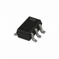
74HC2G17GW,125 NXP Semiconductors, 74HC2G17GW,125 Datasheet - Page 4

74HC2G17GW,125
Manufacturer Part Number
74HC2G17GW,125
Description
IC BUFF DL SCHM TRG N-INV SC88
Manufacturer
NXP Semiconductors
Series
74HCr
Datasheet
1.74HC2G17GW125.pdf
(18 pages)
Specifications of 74HC2G17GW,125
Package / Case
SC-70-6, SC-88, SOT-363
Logic Type
Schmitt Trigger - Buffer, Driver
Number Of Elements
2
Number Of Bits Per Element
1
Current - Output High, Low
5.2mA, 5.2mA
Voltage - Supply
2 V ~ 6 V
Operating Temperature
-40°C ~ 125°C
Mounting Type
Surface Mount
Logic Family
HC
Number Of Channels Per Chip
2
Polarity
Non-Inverting
Supply Voltage (max)
6 V
Supply Voltage (min)
2 V
Maximum Operating Temperature
+ 125 C
Mounting Style
SMD/SMT
High Level Output Current
- 5.2 mA
Low Level Output Current
5.2 mA
Minimum Operating Temperature
- 40 C
Propagation Delay Time
115 ns @ 2 V or 22 ns @ 4.5 V or 18 ns @ 6 V
Number Of Lines (input / Output)
2 / 2
Lead Free Status / RoHS Status
Lead free / RoHS Compliant
Lead Free Status / RoHS Status
Lead free / RoHS Compliant, Lead free / RoHS Compliant
Other names
74HC2G17GW-G
74HC2G17GW-G
935281031125
74HC2G17GW-G
935281031125
Available stocks
Company
Part Number
Manufacturer
Quantity
Price
Part Number:
74HC2G17GW,125
Manufacturer:
NEXPERIA/安世
Quantity:
20 000
NXP Semiconductors
9. Limiting values
Table 5.
In accordance with the Absolute Maximum Rating System (IEC 60134). Voltages are referenced to GND (ground = 0 V).
[1]
[2]
10. Recommended operating conditions
Table 6.
11. Static characteristics
Table 7.
At recommended operating conditions; voltages are referenced to GND (ground = 0 V).
74HC_HCT2G17_1
Product data sheet
Symbol
V
I
I
I
I
I
T
P
Symbol
Type 74HC2G17
V
V
V
T
Type 74HCT2G17
V
V
V
T
Symbol
T
V
IK
OK
O
CC
GND
stg
amb
amb
amb
CC
tot
CC
I
O
CC
I
O
OH
The minimum input and output voltage ratings may be exceeded if the input and output current ratings are observed.
For SC-88 and SC-74 packages: above 87.5 C the value of P
= 25 C
Parameter
supply voltage
input clamping current
output clamping current
output current
supply current
ground current
storage temperature
total power dissipation
Limiting values
Recommended operating conditions
Static characteristics for 74HC2G17
Parameter
HIGH-level output voltage
Parameter
supply voltage
input voltage
output voltage
ambient temperature
supply voltage
input voltage
output voltage
ambient temperature
Conditions
V
I
I
I
I
I
I
Conditions
V
V
V
= V
O
O
O
O
O
I
O
O
Rev. 01 — 6 October 2006
= 20 A; V
= 20 A; V
= 20 A; V
= 4.0 mA; V
= 5.2 mA; V
< 0.5 V or V
< 0.5 V or V
= 0.5 V to V
IH
or V
Conditions
IL
tot
derates linearly with 4.0 mW/K.
CC
CC
CC
CC
CC
I
CC
O
> V
= 2.0 V
= 4.5 V
= 6.0 V
= 4.5 V
= 6.0 V
> V
+ 0.5 V
74HC2G17; 74HCT2G17
CC
CC
+ 0.5 V
+ 0.5 V
Dual non-inverting Schmitt trigger
Min
1.9
4.4
5.9
4.18
5.68
Min
2.0
0
0
4.5
0
0
40
40
Typ
2.0
4.5
6.0
4.32
5.81
Typ
5.0
-
-
+25
5.0
-
-
+25
[1]
[1]
[1]
[1]
[1]
[2]
Min
-
-
-
-
-
-
0.5
65
© NXP B.V. 2006. All rights reserved.
Max
-
-
-
-
-
Max
6.0
V
V
+125
5.5
V
V
+125
CC
CC
CC
CC
Max
+7.0
50
+150
250
20
20
25
50
Unit
V
V
V
V
V
V
C
C
Unit
V
mA
mA
mA
mA
mA
mW
Unit
V
V
V
V
V
4 of 18
C


