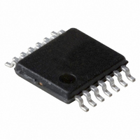
74LV125DB,112 NXP Semiconductors, 74LV125DB,112 Datasheet - Page 5

74LV125DB,112
Manufacturer Part Number
74LV125DB,112
Description
IC BUFF DVR TRI-ST QUAD 14SSOP
Manufacturer
NXP Semiconductors
Series
74LVr
Datasheet
1.74LV125N112.pdf
(15 pages)
Specifications of 74LV125DB,112
Package / Case
14-SSOP
Logic Type
Buffer/Line Driver, Non-Inverting
Number Of Elements
4
Number Of Bits Per Element
1
Current - Output High, Low
16mA, 16mA
Voltage - Supply
1 V ~ 5.5 V
Operating Temperature
-40°C ~ 125°C
Mounting Type
Surface Mount
Logic Family
LV
Number Of Channels Per Chip
4
Polarity
Non-Inverting
Supply Voltage (max)
5.5 V
Supply Voltage (min)
1 V
Maximum Operating Temperature
+ 125 C
Mounting Style
SMD/SMT
High Level Output Current
- 16 mA
Input Bias Current (max)
160 uA
Low Level Output Current
16 mA
Minimum Operating Temperature
- 40 C
Output Type
3-State
Propagation Delay Time
55 ns (Typ) @ 1.2 V or 19 ns (Typ) @ 2 V or 14 ns (Typ) @ 2.7 V or 10 ns (Typ) @ 3.3 V
Number Of Lines (input / Output)
4 / 4
Lead Free Status / RoHS Status
Lead free / RoHS Compliant
Lead Free Status / RoHS Status
Lead free / RoHS Compliant, Lead free / RoHS Compliant
Other names
74LV125DB
74LV125DB
935170160112
74LV125DB
935170160112
NXP Semiconductors
Table 6.
At recommended operating conditions. Voltages are referenced to GND (ground = 0 V).
[1]
10. Dynamic characteristics
Table 7.
Voltages are referenced to GND (ground = 0 V). For test circuit see
74LV125_3
Product data sheet
Symbol Parameter
V
I
I
I
C
Symbol Parameter
t
t
I
OZ
CC
pd
en
I
OL
I
CC
Typical values are measured at T
LOW-level output voltage
input leakage current
OFF-state output current
supply current
additional supply current
input capacitance
propagation delay
enable time
Static characteristics
Dynamic characteristics
Conditions
nA to nY; see
V
V
V
V
V
V
nOE to nY; see
V
V
V
V
V
CC
CC
CC
CC
CC
CC
CC
CC
CC
CC
CC
amb
= 1.2 V
= 2.0 V
= 2.7 V
= 3.0 V to 3.6 V; C
= 3.0 V to 3.6 V
= 4.5 V to 5.5 V
= 1.2 V
= 2.0 V
= 2.7 V
= 3.0 V to 3.6 V
= 4.5 V to 5.5 V
…continued
= 25 C.
Conditions
V
V
V
V
V
V
V
V
per input; V
V
I
I
CC
I
O
CC
I
CC
CC
I
I
I
I
I
I
I
= V
= V
= V
= V
O
O
O
O
O
O
O
= V
= 5.5 V
= 5.5 V
= 5.5 V
= 2.7 V to 3.6 V
= 100 A; V
= 100 A; V
= 100 A; V
= 100 A; V
= 100 A; V
= 8 mA; V
= 16 mA; V
Figure 6
IH
CC
IH
CC
CC
Figure 7
or V
or V
or GND;
or GND; I
or GND;
I
Rev. 03 — 7 April 2009
IL
IL
= V
;
L
CC
= 15 pF
CC
CC
CC
CC
CC
CC
CC
= 3.0 V
O
= 4.5 V
= 1.2 V
= 2.0 V
= 2.7 V
= 3.0 V
= 4.5 V
= 0 A;
0.6 V;
[2]
[3]
[3]
[2]
[3]
Figure
Min
-
-
-
-
-
-
-
-
-
-
-
Min
40 C to +85 C
-
-
-
-
-
-
-
-
-
-
-
-
8.
40 C to +85 C
Typ
Typ
55
19
14
10
75
26
19
14
9
0.20
0.35
-
-
3.5
[1]
0
0
0
0
0
-
-
-
-
[1]
Max
Quad buffer/line driver; 3-state
24
18
14
12
31
23
18
15
-
-
-
Max
0.40
0.55
500
0.2
0.2
0.2
0.2
1.0
20
5
-
-
Min
40 C to +125 C
40 C to +125 C Unit
-
-
-
-
-
-
-
-
-
-
-
Min
-
-
-
-
-
-
-
-
-
-
-
-
© NXP B.V. 2009. All rights reserved.
74LV125
Max
Max
0.50
0.65
31
23
18
15
39
29
23
19
160
850
0.2
0.2
0.2
0.2
1.0
10
-
-
-
-
-
V
V
V
V
V
V
V
pF
5 of 15
Unit
ns
ns
ns
ns
ns
ns
ns
ns
ns
ns
ns
A
A
A
A


