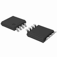
74AHC2G241DP,125 NXP Semiconductors, 74AHC2G241DP,125 Datasheet - Page 8

74AHC2G241DP,125
Manufacturer Part Number
74AHC2G241DP,125
Description
IC BUFF DVR TRI-ST DL 8TSSOP
Manufacturer
NXP Semiconductors
Series
74AHCr
Datasheet
1.74AHC2G241DP125.pdf
(16 pages)
Specifications of 74AHC2G241DP,125
Logic Type
Buffer/Line Driver, Non-Inverting
Number Of Elements
2
Number Of Bits Per Element
1
Current - Output High, Low
8mA, 8mA
Voltage - Supply
2 V ~ 5.5 V
Operating Temperature
-40°C ~ 125°C
Mounting Type
Surface Mount
Package / Case
8-TSSOP
Logic Family
AHC
Number Of Channels Per Chip
2
Polarity
Non-Inverting
Supply Voltage (max)
5.5 V
Supply Voltage (min)
2 V
Maximum Operating Temperature
+ 125 C
Mounting Style
SMD/SMT
High Level Output Current
- 8 mA
Low Level Output Current
8 mA
Minimum Operating Temperature
- 40 C
Number Of Lines (input / Output)
2 / 2
Output Type
3-State
Propagation Delay Time
11.5 ns at 3.3 V, 7.5 ns at 5 V
Lead Free Status / RoHS Status
Lead free / RoHS Compliant
Other names
74AHC2G241DP-G
74AHC2G241DP-G
935274603125
74AHC2G241DP-G
935274603125
NXP Semiconductors
12. Waveforms
74AHC_AHCT2G241_2
Product data sheet
Fig 5.
Fig 6.
Measurement points are given in
Logic levels: V
The input (nA) to output (nY) propagation delays
Measurement points are given in
Logic levels: V
The input (1OE) to output 1Y enable and disable times
OL
OL
and V
and V
HIGH-to-OFF
OFF-to-HIGH
LOW-to-OFF
OFF-to-LOW
1OE input
output
output
OH
OH
are typical output voltage levels that occur with the output load.
are typical output voltage levels that occur with the output load.
nY output
nA input
GND
GND
V
V
V
Table
Table
CC
OH
OL
V
I
9.
9.
GND
V
V
OH
OL
V
I
Rev. 02 — 13 January 2009
V
M
enabled
outputs
t
PLZ
t
PHZ
74AHC2G241; 74AHCT2G241
V
M
V
V
OL
M
V
t
OH
PHL
0.3 V
0.3 V
disabled
outputs
t
PZL
t
PZH
mna230
t
PLH
V
M
V
M
Dual buffer/line driver; 3-state
outputs
enabled
001aaa411
© NXP B.V. 2009. All rights reserved.
8 of 16


