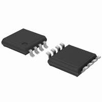
74AHCT2G126DP,125 NXP Semiconductors, 74AHCT2G126DP,125 Datasheet - Page 5

74AHCT2G126DP,125
Manufacturer Part Number
74AHCT2G126DP,125
Description
IC BUFF DVR TRI-ST DL 8TSSOP
Manufacturer
NXP Semiconductors
Series
74AHCTr
Datasheet
1.74AHC2G126DP125.pdf
(16 pages)
Specifications of 74AHCT2G126DP,125
Package / Case
8-TSSOP
Logic Type
Buffer/Line Driver, Non-Inverting
Number Of Elements
2
Number Of Bits Per Element
1
Current - Output High, Low
8mA, 8mA
Voltage - Supply
4.5 V ~ 5.5 V
Operating Temperature
-40°C ~ 125°C
Mounting Type
Surface Mount
Logic Family
AHCT
Number Of Channels Per Chip
2
Polarity
Non-Inverting
Supply Voltage (max)
5.5 V
Supply Voltage (min)
4.5 V
Maximum Operating Temperature
+ 125 C
Mounting Style
SMD/SMT
High Level Output Current
- 8 mA
Input Bias Current (max)
1 uA
Low Level Output Current
8 mA
Maximum Power Dissipation
250 mW
Minimum Operating Temperature
- 40 C
Output Current
25 mA
Output Type
3-State
Propagation Delay Time
7.5 ns @ 4.5 V to 5.5 V
Number Of Lines (input / Output)
2 / 2
Lead Free Status / RoHS Status
Lead free / RoHS Compliant
Lead Free Status / RoHS Status
Lead free / RoHS Compliant, Lead free / RoHS Compliant
Other names
74AHCT2G126DP-G
74AHCT2G126DP-G
935274671125
74AHCT2G126DP-G
935274671125
NXP Semiconductors
Table 7.
Voltages are referenced to GND (ground = 0 V).
11. Dynamic characteristics
Table 8.
GND = 0 V; for test circuit see
74AHC_AHCT2G126
Product data sheet
Symbol Parameter
C
74AHCT2G126
V
V
V
V
I
I
I
I
C
Symbol Parameter
74AHC2G126
t
OZ
I
CC
pd
IH
IL
OH
OL
I
I
CC
input
capacitance
HIGH-level
input voltage
LOW-level
input voltage
HIGH-level
output voltage
LOW-level
output voltage
OFF-state
output current
input leakage
current
supply current V
additional
supply current
input
capacitance
propagation
delay
Static characteristics
Dynamic characteristics
Conditions
nA to nY; see
Conditions
V
V
V
V
V
V
V
V
V
per input pin; V
other inputs at V
I
O
V
V
CC
CC
I
I
I
CC
I
CC
I
CC
I
I
I
I
CC
CC
= V
= V
= V
= 5.5 V or GND;
= V
= 0 A; V
O
O
O
O
C
C
C
C
= 4.5 V to 5.5 V
= 4.5 V to 5.5 V
Figure
= 5.5 V
= 0 V to 5.5 V
= 5.5 V
L
L
L
L
= 50 A
= 8.0 mA
= 50 A
= 8.0 mA
= 3.0 V to 3.6 V
= 4.5 V to 5.5 V
IH
IH
CC
CC
= 15 pF
= 50 pF
= 15 pF
= 50 pF
or V
or V
…continued
or GND;
or GND; I
CC
8.
IL
IL
Figure 6
= 5.5 V
; V
; V
I
= 3.4 V;
All information provided in this document is subject to legal disclaimers.
CC
CC
CC
O
or GND;
= 4.5 V
= 4.5 V
= 0 A;
Rev. 5 — 24 March 2011
[1]
[2]
[3]
74AHC2G126; 74AHCT2G126
-
2.0
-
4.4
3.94
-
-
-
-
-
-
-
Min
Min
-
-
-
-
25 C
25 C
1.5
-
-
4.5
-
0
-
-
-
-
-
1.5
Typ
Typ
4.7
6.6
3.4
4.8
10
-
0.8
-
-
0.1
0.36
0.25
0.1
1.0
1.35
10
Max
Max
11.5
8.0
5.5
7.5
-
4.4
-
-
-
-
-
-
-
2.0
-
3.8
40 C to +85 C 40 C to +125 C Unit
40 C to +85 C 40 C to +125 C Unit
Min
Min
1.0
1.0
1.0
1.0
10
-
0.8
-
-
0.1
0.44
2.5
1.0
10
1.5
10
Dual buffer/line driver; 3-state
Max
13.0
Max
9.5
6.5
8.5
-
2.0
-
4.4
3.70
-
-
-
-
-
-
-
Min
Min
1.0
1.0
1.0
1.0
© NXP B.V. 2011. All rights reserved.
10
-
0.8
-
-
0.1
0.55
10
2.0
40
1.5
10
Max
14.5
Max
11.5
7.0
9.5
5 of 16
pF
V
V
V
V
V
V
A
A
A
mA
pF
ns
ns
ns
ns


