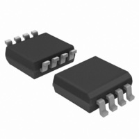
74LVC2G241DC,125 NXP Semiconductors, 74LVC2G241DC,125 Datasheet - Page 8

74LVC2G241DC,125
Manufacturer Part Number
74LVC2G241DC,125
Description
IC BUFF DVR TRI-ST DL INV 8VSSOP
Manufacturer
NXP Semiconductors
Series
74LVCr
Datasheet
1.74LVC2G241DC125.pdf
(23 pages)
Specifications of 74LVC2G241DC,125
Package / Case
US8, 8-VSSOP
Logic Type
Buffer/Line Driver, Non-Inverting
Number Of Elements
2
Number Of Bits Per Element
1
Current - Output High, Low
32mA, 32mA
Voltage - Supply
2 V ~ 5.5 V
Operating Temperature
-40°C ~ 125°C
Mounting Type
Surface Mount
Logic Family
LVC
Number Of Channels Per Chip
2
Polarity
Non-Inverting
Supply Voltage (max)
5.5 V
Supply Voltage (min)
1.65 V
Maximum Operating Temperature
+ 125 C
Mounting Style
SMD/SMT
High Level Output Current
- 32 mA
Input Bias Current (max)
40 uA
Low Level Output Current
32 mA
Maximum Power Dissipation
300 mW
Minimum Operating Temperature
- 40 C
Output Current
50 mA
Output Type
3-State
Output Voltage
6.5 V
Propagation Delay Time
2.8 ns (Typ) @ 2.7 V or 2.6 ns (Typ) @ 3 V to 3.6 V or 2.1 ns (Typ) @ 4.5 V to 5.5 V
Number Of Lines (input / Output)
2 / 2
Lead Free Status / RoHS Status
Lead free / RoHS Compliant
Lead Free Status / RoHS Status
Lead free / RoHS Compliant, Lead free / RoHS Compliant
Other names
74LVC2G241DC-G
74LVC2G241DC-G
935274509125
74LVC2G241DC-G
935274509125
NXP Semiconductors
11. Dynamic characteristics
Table 8.
Voltages are referenced to GND (ground = 0 V); for test circuit see
74LVC2G241
Product data sheet
Symbol Parameter
t
t
t
pd
en
dis
propagation delay nA to nY; see
enable time
disable time
Dynamic characteristics
Conditions
1OE to 1Y; see
2OE to 2Y; see
1OE to 1Y; see
2OE to 2Y; see
V
V
V
V
V
V
V
V
V
V
V
V
V
V
V
V
V
V
V
V
V
V
V
V
V
CC
CC
CC
CC
CC
CC
CC
CC
CC
CC
CC
CC
CC
CC
CC
CC
CC
CC
CC
CC
CC
CC
CC
CC
CC
= 1.65 V to 1.95 V
= 2.3 V to 2.7 V
= 2.7 V
= 3.0 V to 3.6 V
= 4.5 V to 5.5 V
= 1.65 V to 1.95 V
= 2.3 V to 2.7 V
= 2.7 V
= 3.0 V to 3.6 V
= 4.5 V to 5.5 V
= 1.65 V to 1.95 V
= 2.3 V to 2.7 V
= 2.7 V
= 3.0 V to 3.6 V
= 4.5 V to 5.5 V
= 1.65 V to 1.95 V
= 2.3 V to 2.7 V
= 2.7 V
= 3.0 V to 3.6 V
= 4.5 V to 5.5 V
= 1.65 V to 1.95 V
= 2.3 V to 2.7 V
= 2.7 V
= 3.0 V to 3.6 V
= 4.5 V to 5.5 V
All information provided in this document is subject to legal disclaimers.
Figure 7
Figure 8
Figure 9
Figure 8
Figure 9
Rev. 10 — 6 August 2010
[2]
[3]
[3]
[4]
[4]
Figure
Min
1.0
0.5
1.0
0.5
0.5
1.5
1.0
1.5
0.5
0.5
1.0
1.0
1.0
1.0
0.5
1.0
0.5
1.0
1.0
0.5
1.0
0.5
1.5
1.0
0.5
−40 °C to +85 °C
10.
Typ
4.5
2.8
2.8
2.6
2.1
5.2
3.1
3.2
2.7
2.0
4.3
2.7
2.7
2.5
1.9
3.2
2.2
2.8
2.6
2.0
3.6
2.0
3.2
2.8
2.0
[1]
Dual buffer/line driver; 3-state
Max
11.6
12.5
8.8
4.9
4.7
4.3
3.7
9.9
5.6
5.5
4.7
3.8
8.8
4.7
4.6
4.1
3.3
5.8
4.6
4.4
3.4
5.2
4.9
4.2
3.3
74LVC2G241
−40 °C to +125 °C Unit
Min
1.0
0.5
1.0
0.5
0.5
1.5
1.0
1.5
0.5
0.5
1.0
1.0
1.0
1.0
0.5
1.0
0.5
1.0
1.0
0.5
1.0
0.5
1.5
1.0
0.5
© NXP B.V. 2010. All rights reserved.
Max
11.0
12.4
11.0
14.1
15.2
6.3
5.9
5.4
4.6
7.0
6.9
5.9
4.8
5.9
5.8
5.1
4.1
7.6
5.9
5.7
4.6
6.9
6.3
5.4
4.4
ns
ns
ns
ns
ns
ns
ns
ns
ns
ns
ns
ns
ns
ns
ns
ns
ns
ns
ns
ns
ns
ns
ns
ns
ns
8 of 23


