N74F541N,602 NXP Semiconductors, N74F541N,602 Datasheet - Page 5
N74F541N,602
Manufacturer Part Number
N74F541N,602
Description
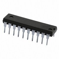
IC BUFF/DVR TRI-ST 8BIT 20DIP
Manufacturer
NXP Semiconductors
Series
74Fr
Datasheet
1.N74F541N602.pdf
(10 pages)
Specifications of N74F541N,602
Logic Type
Buffer/Line Driver, Non-Inverting
Number Of Elements
1
Number Of Bits Per Element
8
Current - Output High, Low
15mA, 64mA
Voltage - Supply
4.5 V ~ 5.5 V
Operating Temperature
0°C ~ 70°C
Mounting Type
Through Hole
Package / Case
20-DIP (0.300", 7.62mm)
Lead Free Status / RoHS Status
Lead free / RoHS Compliant
Other names
933769310602
N74F541N
N74F541N
N74F541N
N74F541N


1. For conditions shown as MIN or MAX, use the appropriate value under the recommended operating conditions for the applicable type.
2. All typical values are at V
3. Not more than one output should be shorted at a time. For testing I
Philips Semiconductors
DC ELECTRICAL CHARACTERISTICS
(Over recommended operating free-air temperature range unless otherwise noted.)
NOTES:
1990 Jan 08
SYMBOL
V
V
V
V
V
I
I
I
I
I
I
I
I
I
IH
IL
OZH
OZL
OS
CC
CC
Buffers
techniques are preferable in order to minimize internal heating and more accurately reflect operational values. Otherwise, prolonged shorting
of a High output may raise the chip temperature well above normal and thereby cause invalid readings in other parameter tests. In any
sequence of parameter tests, I
O
OH
O
OL
IK
High level output voltage
High-level output voltage
Low level output voltage
Low-level output voltage
Input clamp voltage
Input current at maximum input
voltage
High-level input current
Low-level input current
Off-state output current
High-level voltage applied
Off-state output current
Low-level voltage applied
Short-circuit output current
Supply current
(total)
y
PARAMETER
CC
= 5V, T
OS
74F540
74F541
should be performed last.
amb
NO TAG
= 25 C.
I
I
I
I
I
I
CCH
CCH
CCL
CCZ
CCL
CCZ
V
V
V
V
V
V
V
V
V
V
CC
CC
IL
IL
CC
CC
IL
IL
IH
IH
= MAX
= MAX,
= MAX
= MAX,
= MIN,
= MIN,
= MIN
= MIN
= MAX
= MAX
TEST CONDITIONS
V
V
V
V
V
CC
CC
CC
CC
CC
V
CC
= MAX, V
= MAX, V
= MAX, V
= MAX, V
= 0.0V, V
V
OS
= MIN, I
CC
I
I
In=OEn=GND
In=4.5V, OEn=GND
In=GND, OEn=4.5V
In=4.5V, OEn=GND
In=OEn=GND
In=GND, OEn=4.5V
5
I
I
O
OH
O
OH
I
I
, the use of high-speed test apparatus and/or sample-and-hold
O
OL
= MAX
= 15mA
= –15mA
= 3mA
= –3mA
= MAX
= MAX
O
O
I
I
I
I
= 7.0V
= 2.7V
= 0.5V
= I
= 2.7V
= 0.5V
NO TAG
NO TAG
IK
10%V
10%V
10%V
5%V
5%V
5%V
CC
CC
CC
CC
CC
CC
–100
MIN
2.4
2.7
2.0
2.0
LIMITS
NO TAG
–0.73
74F540, 74F541
TYP
0.42
3.4
22
58
40
30
55
45
MAX
–225
0.55
0.55
–1.2
100
–20
–50
20
30
75
55
40
72
58
50
Product specification
UNIT
mA
mA
mA
mA
mA
mA
mA
V
V
V
V
V
V
V
A
A
A
A
A
Related parts for N74F541N,602
Image
Part Number
Description
Manufacturer
Datasheet
Request
R

Part Number:
Description:
Buffers & Line Drivers OCTAL 3-ST DRV/BUF
Manufacturer:
NXP Semiconductors
Part Number:
Description:
NXP Semiconductors designed the LPC2420/2460 microcontroller around a 16-bit/32-bitARM7TDMI-S CPU core with real-time debug interfaces that include both JTAG andembedded trace
Manufacturer:
NXP Semiconductors
Datasheet:

Part Number:
Description:
NXP Semiconductors designed the LPC2458 microcontroller around a 16-bit/32-bitARM7TDMI-S CPU core with real-time debug interfaces that include both JTAG andembedded trace
Manufacturer:
NXP Semiconductors
Datasheet:
Part Number:
Description:
NXP Semiconductors designed the LPC2468 microcontroller around a 16-bit/32-bitARM7TDMI-S CPU core with real-time debug interfaces that include both JTAG andembedded trace
Manufacturer:
NXP Semiconductors
Datasheet:
Part Number:
Description:
NXP Semiconductors designed the LPC2470 microcontroller, powered by theARM7TDMI-S core, to be a highly integrated microcontroller for a wide range ofapplications that require advanced communications and high quality graphic displays
Manufacturer:
NXP Semiconductors
Datasheet:
Part Number:
Description:
NXP Semiconductors designed the LPC2478 microcontroller, powered by theARM7TDMI-S core, to be a highly integrated microcontroller for a wide range ofapplications that require advanced communications and high quality graphic displays
Manufacturer:
NXP Semiconductors
Datasheet:
Part Number:
Description:
The Philips Semiconductors XA (eXtended Architecture) family of 16-bit single-chip microcontrollers is powerful enough to easily handle the requirements of high performance embedded applications, yet inexpensive enough to compete in the market for hi
Manufacturer:
NXP Semiconductors
Datasheet:
Part Number:
Description:
The XA-S3 device is a member of Philips Semiconductors? XA(eXtended Architecture) family of high performance 16-bitsingle-chip microcontrollers
Manufacturer:
NXP Semiconductors
Datasheet:

Part Number:
Description:
The NXP BlueStreak LH75401/LH75411 family consists of two low-cost 16/32-bit System-on-Chip (SoC) devices
Manufacturer:
NXP Semiconductors
Datasheet:
Part Number:
Description:
The NXP LPC3130/3131 combine an 180 MHz ARM926EJ-S CPU core, high-speed USB2
Manufacturer:
NXP Semiconductors
Datasheet:
Part Number:
Description:
The NXP LPC3141 combine a 270 MHz ARM926EJ-S CPU core, High-speed USB 2
Manufacturer:
NXP Semiconductors
Part Number:
Description:
The NXP LPC3143 combine a 270 MHz ARM926EJ-S CPU core, High-speed USB 2
Manufacturer:
NXP Semiconductors

Part Number:
Description:
The NXP LPC3152 combines an 180 MHz ARM926EJ-S CPU core, High-speed USB 2
Manufacturer:
NXP Semiconductors
Part Number:
Description:
The NXP LPC3154 combines an 180 MHz ARM926EJ-S CPU core, High-speed USB 2
Manufacturer:
NXP Semiconductors