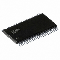
74ALVCH162245DGG:5 NXP Semiconductors, 74ALVCH162245DGG:5 Datasheet - Page 2

74ALVCH162245DGG:5
Manufacturer Part Number
74ALVCH162245DGG:5
Description
IC TRANSCVR 16BIT N-INV 48TSSOP
Manufacturer
NXP Semiconductors
Series
74ALVCHr
Datasheet
1.74ALVCH162245DGG5.pdf
(11 pages)
Specifications of 74ALVCH162245DGG:5
Logic Type
Transceiver, Non-Inverting
Number Of Elements
2
Number Of Bits Per Element
8
Current - Output High, Low
12mA, 12mA
Voltage - Supply
2.3 V ~ 3.6 V
Operating Temperature
-40°C ~ 85°C
Mounting Type
Surface Mount
Package / Case
48-TSSOP
Lead Free Status / RoHS Status
Lead free / RoHS Compliant
Other names
74ALVCH162245DG-T
74ALVCH162245DG-T
935210840518
74ALVCH162245DG-T
935210840518
1. C
Philips Semiconductors
FEATURES
DESCRIPTION
The 74ALVCH162245 is a 16-bit transceiver featuring non-inverting
3-State bus compatible outputs in both send and receive directions.
The 74ALVCH162245 features two output enable (nOE) inputs for
easy cascading and two send/receive (nDIR) inputs for direction
control. nOE controls the outputs so that the buses are effectively
isolated. This device can be used as two 8-bit transceivers or one
16-bit transceiver.
The 74ALVCH162245 is designed with 30 series resistors in both
HIGH and LOW output states.
The 74ALVCH162245 has active bus hold circuitry which is provided
to hold unused or floating data inputs at a valid logic level. This
feature eliminates the need for external pull-up or pull-down
resistors.
QUICK REFERENCE DATA
GND = 0V; T
NOTES:
ORDERING INFORMATION
48-Pin Plastic SSOP Type III
48-Pin Plastic TSSOP Type II
1998 Jun 29
Wide supply voltage range of 1.2V to 3.6V
Complies with JEDEC standard no. 8-1A
CMOS low power consumption
MULTIBYTE
Low inductance multiple V
and ground bounce
Direct interface with TTL levels
Bus hold on all data inputs
Integrated 30 termination resistor
16-bit bus transceiver with direction pin and
30 termination resistor (3-State)
t
C
C
C
C
PHL
P
f
SYMBOL
o
I
I/O
PD
PD
D
= output frequency in MHz; V
= C
/t
PLH
is used to determine the dynamic power dissipation (P
PD
amb
PACKAGES
TM
V
= 25 C; t
CC
flow-through standard pin-out architecture
Propagation delay
An to Bn; Bn to An
Input capacitance
Input/output capacitance
Power dissipation capacitance per buffer
Power dissipation capacitance per buffer
2
f
i
+ S (C
r
= t
CC
f
L
and ground pins for minimum noise
2.5ns
PARAMETER
V
CC
CC
= supply voltage in V; S (C
2
TEMPERATURE RANGE
f
o
) where: f
–40 C to +85 C
–40 C to +85 C
i
= input frequency in MHz; C
D
in W):
L
V
V
V = GND to V
V
CC
CC
I
= GND to V
OUTSIDE NORTH AMERICA
V
CC
= 2.5V, C
= 3.3V, C
74ALVCH162245 DGG
2
2
74ALVCH162245 DL
PIN CONFIGURATION
f
o
) = sum of the outputs.
L
L
CC
CC
= 30pF
= 50pF
1
1
L
CONDITIONS
= output load capacitance in pF;
V
V
1DIR
GND
GND
GND
GND
2DIR
1B0
1B1
1B2
1B3
1B4
1B5
1B6
1B7
2B0
2B1
2B2
2B3
CC1
2B4
2B5
2B6
2B7
CC1
Outputs disabled
Outputs enabled
10
11
12
13
14
15
16
17
18
19
20
21
22
23
24
1
2
3
4
5
6
7
8
9
NORTH AMERICA
ACH162245 DGG
ACH162245 DL
74ALVCH162245
SW00198
48
47
46
45
44
43
42
41
40
39
38
37
36
35
34
33
32
31
30
29
28
27
26
25
TYPICAL
1OE
1A0
1A1
GND
1A2
1A3
V
1A4
1A5
GND
1A6
1A7
2A0
2A1
GND
2A2
2A3
V
2A4
2A5
GND
2A6
2A7
2OE
Product specification
CC2
CC2
2.4
4.0
8.0
27
4
DWG NUMBER
853-2085 19638
SOT370-1
SOT362-1
UNIT
pF
pF
pF
pF
ns


