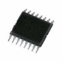
74LV365PW,118 NXP Semiconductors, 74LV365PW,118 Datasheet - Page 6

74LV365PW,118
Manufacturer Part Number
74LV365PW,118
Description
IC BUFF/DVR TRI-ST 6BIT 16TSSOP
Manufacturer
NXP Semiconductors
Series
74LVr
Datasheet
1.74LV365D118.pdf
(12 pages)
Specifications of 74LV365PW,118
Package / Case
16-TSSOP
Logic Type
Buffer/Line Driver, Non-Inverting
Number Of Elements
1
Number Of Bits Per Element
6
Current - Output High, Low
8mA, 8mA
Voltage - Supply
1 V ~ 3.6 V
Operating Temperature
-40°C ~ 125°C
Mounting Type
Surface Mount
Logic Family
LV
Number Of Channels Per Chip
6
Polarity
Non-Inverting
Supply Voltage (max)
3.6 V
Supply Voltage (min)
1 V
Maximum Operating Temperature
+ 125 C
Mounting Style
SMD/SMT
High Level Output Current
- 8 mA
Input Bias Current (max)
160 uA
Low Level Output Current
8 mA
Minimum Operating Temperature
- 40 C
Output Type
3-State
Propagation Delay Time
55 ns (Typ) @ 1.2 V or 19 ns (Typ) @ 2 V or 14 ns (Typ) @ 2.7 V or 10 ns (Typ) @ 3.3 V
Number Of Lines (input / Output)
6 / 6
Lead Free Status / RoHS Status
Lead free / RoHS Compliant
Lead Free Status / RoHS Status
Lead free / RoHS Compliant, Lead free / RoHS Compliant
Other names
74LV365PW-T
74LV365PW-T
935174810118
74LV365PW-T
935174810118
1. All typical values are measured at T
2. Typical values are measured at V
Philips Semiconductors
AC CHARACTERISTICS
GND = 0V; t
NOTES:
AC WAVEFORMS
V
V
V
output load.
V
V
V
V
1998 May 29
SYMBOL
M
M
OL
X
X
Y
Y
t
t
t
t
t
t
PHL/
PZH/
PHZ/
Hex buffer/line driver (3-State)
= V
= V
= V
= V
nY OUTPUT
= 1.5V at V
= 0.5V * V
and V
Figure 1. Input (nA) to output (nY) propagation delays.
nA INPUT
/
/
/
t
t
t
t
t
t
OL
OL
OH
OH
PLH
PZL
PLZ
+ 0.3V at V
+ 0.1V
– 0.3V at V
– 0.1V
OH
V
r
V
OH
= t
OL
are the typical output voltage drop that occur with the
CC
GND
Propagation delay
nA to nY
3-State output
enable time
enable time
OEn to nY
3-State output
disable time
disable time
OEn to nY
V
CC
CC
f
CC
CC
at V
PARAMETER
w 2.7V
2.5ns; C
at V
at V
t
g
PHL
CC
CC
CC
CC
CC
w 2.7V
t 2.7V
w 2.7V
L
2.7V
= 50pF; R
2.7V
V
M
y
V
M
CC
WAVEFORM
amb
L
= 3.3V
= 1KW
Figure 1
Figure 1
Figure 2
Figure 2
Figure 2
Figure 2
= 25 C
SV00648
t
PLH
CONDITION
CONDITION
3.0 to 3.6
3.0 to 3.6
3.0 to 3.6
V
CC
1.2
2.0
2.7
1.2
2.0
2.7
1.2
2.0
2.7
(V)
6
HIGH–to–OFF
OFF–to–HIGH
OEn INPUT
LOW–to–OFF
OFF–to–LOW
OUTPUT
OUTPUT
V
V
CC
OL
GND
GND
V
V
CC
CC
Figure 2. 3-State enable and disable times.
MIN
–
–
–
–
–
–
–
–
–
–
–
–
–40 to +85 C
enabled
outputs
V
TYP
M
t
PLZ
100
t
10
16
21
PHZ
55
19
14
85
29
21
36
27
2
2
2
1
V
LIMITS
X
V
MAX
Y
36
26
21
56
41
33
66
48
39
–
–
–
disabled
outputs
–40 to +125 C
MIN
–
–
–
–
–
–
–
–
–
–
–
–
t
PZL
Product specification
t
PZH
MAX
74LV365
44
33
26
66
49
39
78
58
47
–
–
–
V
M
V
M
SV00649
UNIT
outputs
enabled
ns
ns
ns
ns
ns
ns


